Nonvolatile memory element, nonvolatile memory element array, and method for manufacturing nonvolatile memory element

a technology of memory elements and arrays, applied in semiconductor devices, diodes, electrical apparatus, etc., can solve the problem of not being electrically conductive, and achieve the effect of compact memory cell configuration, reduced resistance variable layer exposed to hydrogen atmosphere, and high current drivability

Active Publication Date: 2010-03-18
PANASONIC SEMICON SOLUTIONS CO LTD
View PDF3 Cites 15 Cited by
  • Summary
  • Abstract
  • Description
  • Claims
  • Application Information

AI Technical Summary

Benefits of technology

[0054]A nonvolatile memory element of the present invention uses a memory cell having a configuration in which a resistance variable element using a resistance variable layer and a rectifying element are connected to each other in series in a stack direction. With this configuration, write disturb, cross talk, and the like from an adjacent memory cell are prevented. Further, to prevent the resistance variable layer from being exposed to a hydrogen atmosphere, a blocking layer disposed on or above the resistance variable layer is formed as a barrier layer having a hydrogen barrier property. With this configuration, the possibility that the resistance variable layer contacts hydrogen decreases, and thus, the resistance variable layer is protected from hydrogen. In a cross-point type nonvolatile memory element suitable for high integration, the rectifying element is connected to resistance variable element in each memory cell to prevent the write disturb of flowing the bypass current from an adjacent memory cell. To further utilize this configuration, an MIM diode or the like having high current drivability is used as the rectifying element, and the barrier layer having the hydrogen barrier property is used as the blocking layer constituting the diode. With this, the possibility that the resistance variable layer is exposed to the hydrogen atmosphere decreases. Further, by forming an electrode layer of the resistance variable element and an electrode layer of the diode as a single layer, the configuration of the memory cell can be made compact and simplified.
[0055]Moreover, when data is not read out from or written to the memory cell in which the resistance variable element and the rectifying element are connected to each other in series, voltage is not applied to the rectifying element. Therefore, the rectifying element is a high-resistance state. On this account, as compared to the memory cell constituted by only the resistance variable element, the resistance variable element can be further protected from electrical noise, and the like. Further, when data is read out from or written to the memory cell, the voltage applied to the memory cell is an applied voltage which has been stably dropped by the rectifying element to have a stable magnitude. Therefore, it is possible to surely prevent unintentional rewriting caused by a high voltage applied to the resistance variable element. Thus, a highly reliable nonvolatile memory element can be realized.
[0056]Moreover, the cross-point type nonvolatile memory element of the present invention can be manufactured by a mass production process compatible with a process adapted for miniaturization in which a process rule of less than 100 nm is main. Since the diode having high current drivability is connected as the rectifying element to the resistance variable element in series, the resistance variable element can stably repeat resistance variation.
[0057]By using the nonvolatile memory element of the present invention, electronic devices, such as portable information equipment and information appliance equipment, can be further reduced in size and thickness and obtain high reliability.

Problems solved by technology

However, the insulating hydrogen barrier layer is not electrically conductive.

Method used


Image

  • Nonvolatile memory element, nonvolatile memory element array, and method for manufacturing nonvolatile memory element
  • Nonvolatile memory element, nonvolatile memory element array, and method for manufacturing nonvolatile memory element
  • Nonvolatile memory element, nonvolatile memory element array, and method for manufacturing nonvolatile memory element

Examples


embodiment 1

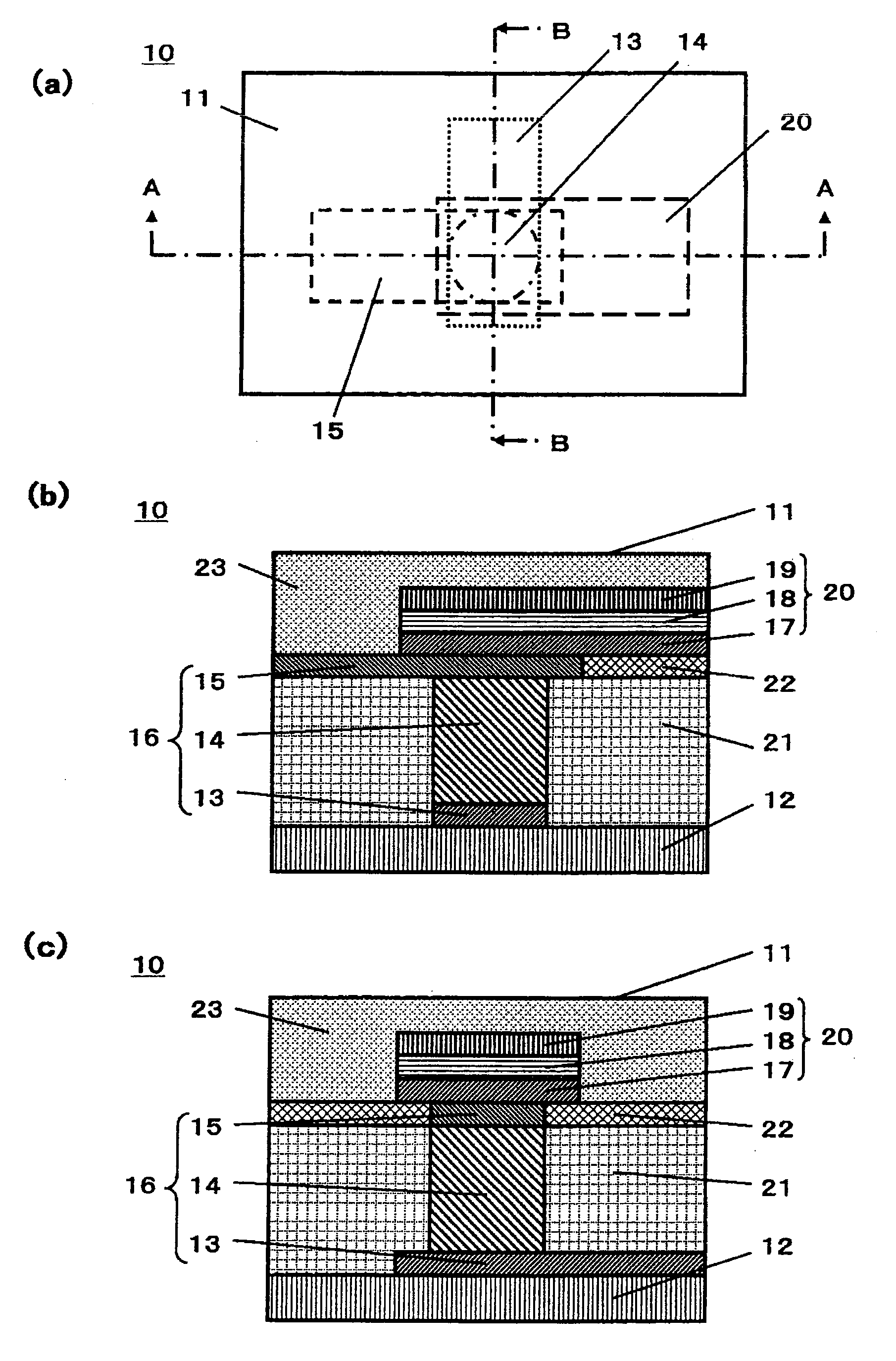
[0101]FIGS. 1 to 7 are diagrams showing Embodiment 1 of the present invention. FIG. 1 are schematic configuration diagrams of a nonvolatile memory element 10 of Embodiment 1 of the present invention. FIG. 1(a) is a schematic diagram showing a schematic configuration of the nonvolatile memory element 10 when viewed from a semiconductor chip surface 11. FIG. 1(b) is a schematic cross-sectional view taken along line A-A of FIG. 1(a) when viewed from a direction indicated by arrows A. FIG. 1(c) is a schematic cross-sectional view taken along line B-B of FIG. 1(a) when viewed from a direction indicated by arrows B.

[0102]In FIG. 1(a), a lower electrode 13 and an upper electrode 15 are disposed to sandwich a resistance variable layer 14 in a stack direction (thickness direction of the resistance variable layer 14; the same is true in the following explanation), and a rectifying element 20 is disposed on the upper electrode 15.

[0103]Moreover, as shown in FIGS. 1(b) and 1(c), the nonvolatile...

embodiment 2

[0138]FIGS. 8 and 9 are diagrams showing Embodiment 2 of the present invention.

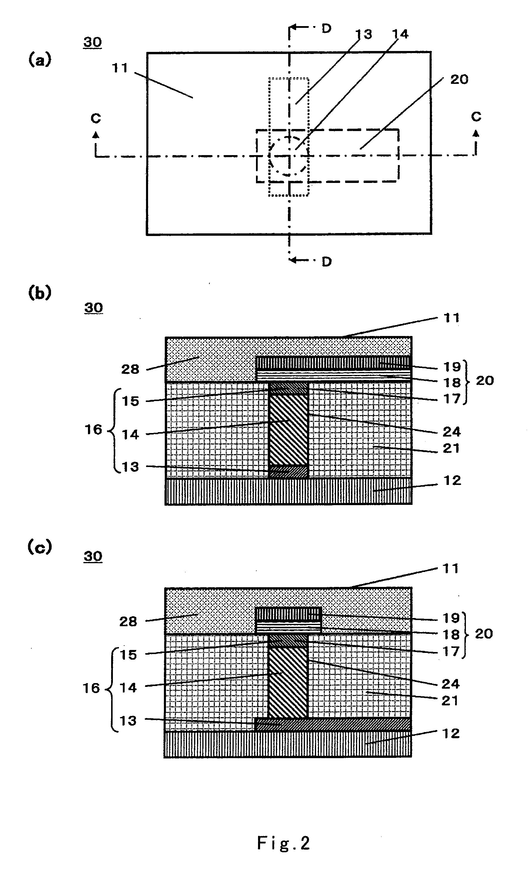
[0139]FIG. 8 is a schematic configuration diagram showing the configuration of a cross-point type nonvolatile memory element array 40 when viewed from a semiconductor chip surface 31. As shown in FIG. 8, the nonvolatile memory element array 40 is configured such that the nonvolatile memory elements 30 of FIG. 2 are arranged as memory cells F in a cross-point manner. To be specific, in FIG. 8, the lower electrode 13 on the substrate (not shown) and the second electrode layer 19 having a stripe shape crossing the lower electrode 13 at right angle herein are configured to sandwich the resistance variable element 16 and the rectifying element 20. With this configuration, the write disturb is prevented, and in addition, the resistance variable element 16 can be driven by high current drivability. To be specific, the rectifying element 20 may be the MIM diode, the MSM diode, or the schottky diode. In this case,...

embodiment 3

[0150]FIG. 10 are schematic configuration diagrams of a nonvolatile memory element 45 of Embodiment 3 of the present invention. FIG. 10(a) is a schematic diagram showing a schematic configuration of the nonvolatile memory element 45 when viewed from a semiconductor chip surface 36. FIG. 10(b) is a schematic cross-sectional view taken along line I-I of FIG. 10(a) when viewed from a direction indicated by arrows I. FIG. 10(c) is a schematic cross-sectional view taken along line J-J of FIG. 10(a) when viewed from a direction indicated by arrows J.

[0151]In the present embodiment, unlike Embodiments 1 and 2, a metal wire layer is further formed on the second electrode layer 19 of the nonvolatile memory element 45 to extend in parallel with the second electrode layer 19. Thus, the wiring resistance of the second electrode layer 19 is practically reduced, and this realizes the increase in speed and the decrease in power consumption.

[0152]To be specific, as shown in FIGS. 10(b) and 10(c), t...


PUM


Abstract

The present invention is configured such that a resistance variable element (16) and a rectifying element (20) are formed on a substrate (12). The resistance variable element (16) is configured such that a resistance variable layer (14) made of a metal oxide material is sandwiched between a lower electrode (13) and an upper electrode (15). The rectifying element (20) is connected to the resistance variable element (16), and is configured such that a blocking layer (18) is sandwiched between a first electrode layer (17) located on a lower side of the blocking layer (18) and a second electrode layer (19) located on an upper side of the blocking layer (18). The resistance variable element (16) and the rectifying element (20) are connected to each other in series in a thickness direction of the resistance variable layer (14), and the blocking layer (18) is formed as a barrier layer having a hydrogen barrier property.

Description

TECHNICAL FIELD[0001]The present invention relates to a nonvolatile memory element suitable for miniaturization and mass production, a nonvolatile memory element array, and a method for manufacturing the nonvolatile memory element.BACKGROUND ART[0002]In recent years, functions of portable digital equipment, such as compact thin digital AV players and digital cameras, have been enhanced, and therefore, there is a growing need for large-capacity high-speed nonvolatile memory elements used as memory elements of the above equipment. To meet the need, a nonvolatile memory element using a ferroelectric capacitor is available.[0003]Many of ferroelectric layers are made of an oxide. Therefore, such memory materials need to be manufactured by a manufacturing process which does not expose the memory materials to a reduction atmosphere, such as a hydrogen atmosphere, and the nonvolatile memory element having an element structure which can be manufactured in such manufacturing process is requir...

Claims


Application Information

Patent Timeline
Patent Type & Authority Applications(United States)
IPC IPC(8): H01L27/10H01L21/02
CPCH01L27/101H01L27/1021H01L45/04H01L45/1233H01L27/2463H01L45/1683H01L27/2409H01L27/2418H01L45/146H10B63/22H10B63/20H10B63/80H10N70/20H10N70/826H10N70/8833H10N70/066
Inventor TAKAGI, TAKESHIMIKAWA, TAKUMI
Owner PANASONIC SEMICON SOLUTIONS CO LTD
Why Eureka
Try Eureka