Nano-hole array in conductor element for improving the contact conductance

a conductor element and nano-hole technology, applied in the direction of conductors, conductive layers on insulating supports, basic electric elements, etc., can solve the problems of ineffective enhancement of contact conductivity of junctions by art, and achieve the effect of improving thermal conduction and high contact conductivity of interfaces

Active Publication Date: 2010-03-25
NAT TAIWAN UNIV
View PDF15 Cites 2 Cited by
  • Summary
  • Abstract
  • Description
  • Claims
  • Application Information

AI Technical Summary

Benefits of technology

[0020]Given the modification of the surfaces of the layers, the nano-hole array of the present invention is capable of providing higher contact conductivity of the interfaces between the conductor elements, because of periodic nano-hole configuration and the area ratio of the nano-hole array to the first layer. Unlike the prior art that taught changing contact conductance by performing rapid thermal annealing at high temperature, the present invention also discloses changing contact conductance by performing rapid thermal annealing at low temperature merely whether on a component or integrated circuit (IC). Furthermore, the aluminum film layer of the present invention is formed with a cladding layer of crystalline grain having better thermal conduction than amorphous structure.

Problems solved by technology

However, the prior art fails to enhance contact conductivity of the junctions efficiently.

Method used


Image

  • Nano-hole array in conductor element for improving the contact conductance
  • Nano-hole array in conductor element for improving the contact conductance
  • Nano-hole array in conductor element for improving the contact conductance

Examples


Embodiment Construction

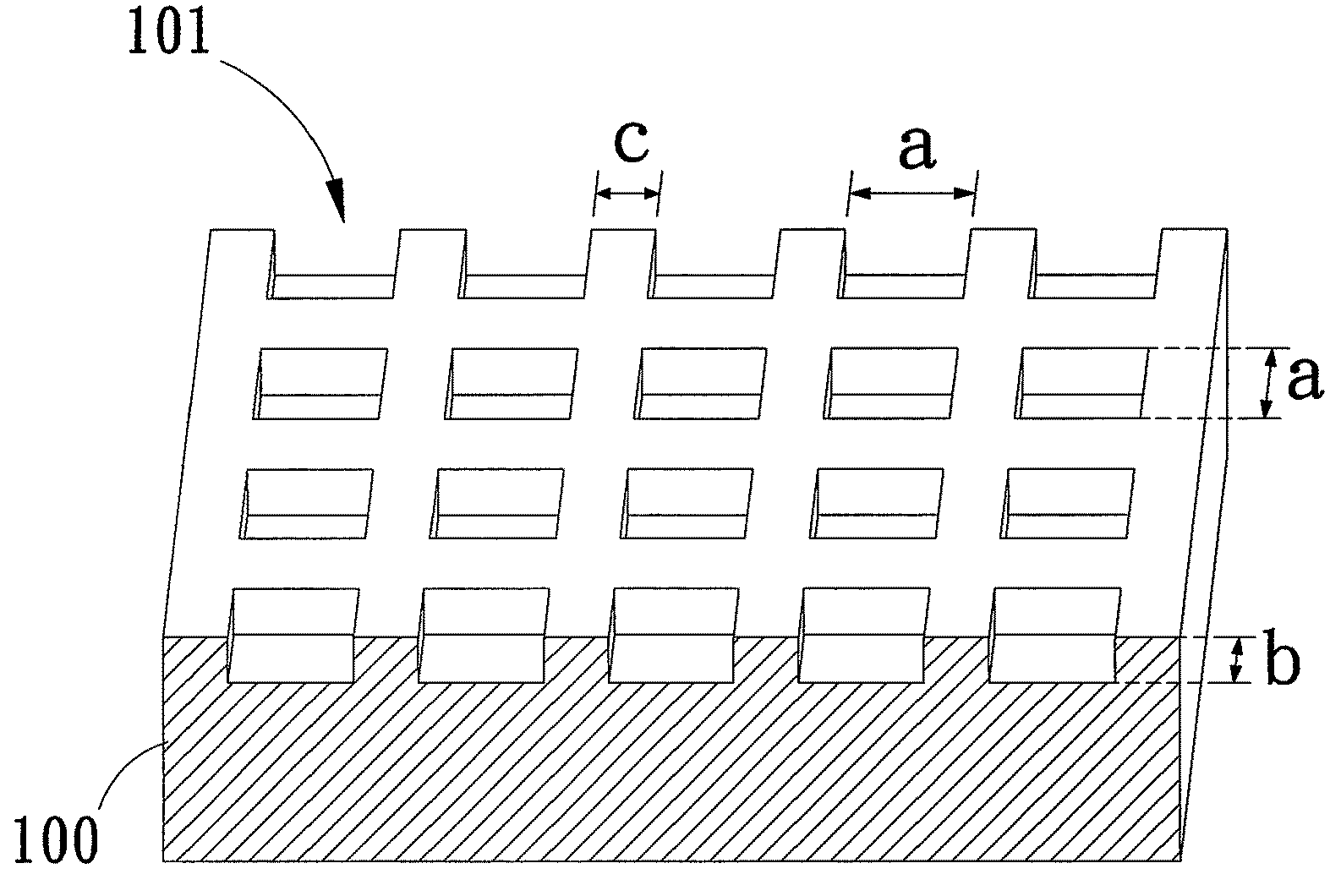
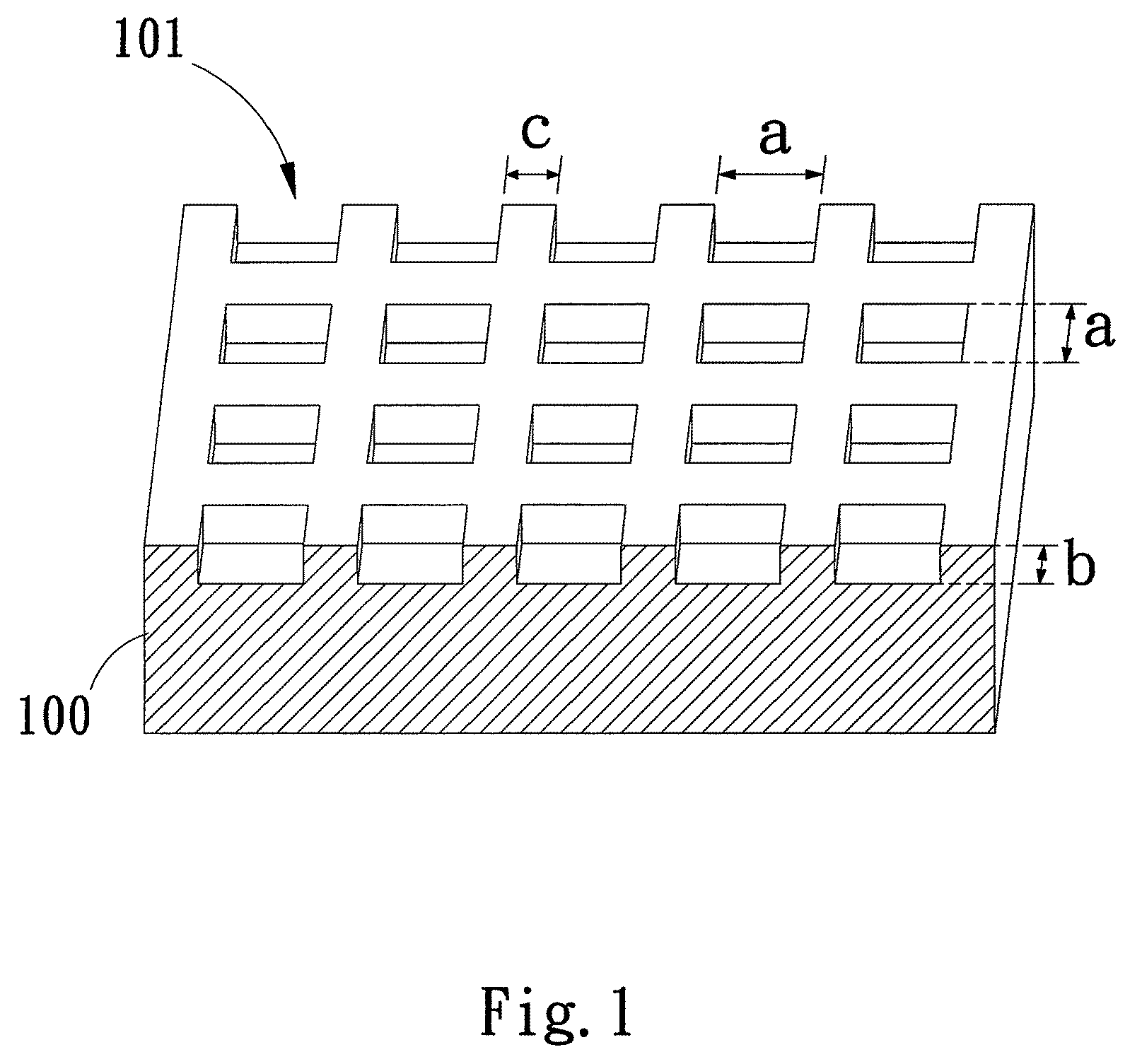
[0025]The objectives, features, and effects of the present invention will be best understood by the reference to the following detailed description of the preferred embodiments when read in conjunction with the accompanying drawings. A nano-hole array of the present invention is formed on a first layer of a conductor element so as to function as an interface. Forming the nano-hole array of the present invention comprises the formation of the periodic nano-hole array configuration on the first layer of the conductor element by conventional semiconductor technique and then the formation of a second layer on top of the nano-hole array. The first layer and the second layer are made of semiconductor material or metal. The semiconductor materials are silicon (Si), germanium (Ge), or group II-V compound-based semiconductors. The metals are titanium (Ti), aluminum (Al), nickel (Ni), copper (Cu), indium (In), magnesium (Mg), or platinum (Pt). Contact conductivity is enhanced by the nano-hole...


PUM

PropertyMeasurementUnit
side lengthaaaaaaaaaa
distanceaaaaaaaaaa

Abstract

A nano-hole array for improving contact conductance of a conductor element that consists of a first layer and a second layer is provided. The nano-hole array formed between the first and second layers comprises a plurality of holes. The contact conductance of the conductor element is enhanced by reducing the hole size of the hole array, increasing the occupation rate of the hole array, and performing thermal annealing.

Description

BACKGROUND OF THE INVENTION[0001]1. Field of the Invention[0002]The present invention relates to a nano-hole array, and more particularly, to a nano-hole array for improving contact conductance of an interface for a conductor element.[0003]2. Description of the Prior Art[0004]In the field of semiconductor components, metal-semiconductor ohmic contacts play an important role in component-to-component bridging and component-to-outside bridging. A junction is good enough to function as an ohmic contact only if the junction leaves the operating characteristics of a component unchanged, provides the component with required current at applied voltage, and exhibits a low junction-voltage-drop to operating-component-voltage-drop ratio. Regarding component application, an ohmic contact is vitally important to a semiconductor component fabrication process, as an ohmic contact is a factor in the contact conductivity of the metal semiconductor junction.[0005]Junction resistance at an interface ...

Claims


Application Information

Patent Timeline
Patent Type & Authority Applications(United States)
IPC IPC(8): H01B5/00
CPCH01L21/283H01L23/3677H01L23/485H01L29/0657H01L29/41H01L29/456Y10S977/784H01L2924/0002Y10S977/755H01L2924/00
Inventor LI, JONG-LIHKUAN, CHIEH-HSIUNG
Owner NAT TAIWAN UNIV
Why Eureka
Try Eureka