

Organic electroluminescent display device and patterning method
a display device and electroluminescent technology, applied in the manufacture of electrode systems, electric discharge tubes/lamps, instruments, etc., can solve the problems of poor heat resistance, reduced electric current value, and difficulty in directly forming silicon thin films on resin substrates, and achieve high field-effect mobility, high on/off ratio, and the ability to control a high electric current
- Summary
- Abstract
- Description
- Claims
- Application Information
AI Technical Summary
Benefits of technology
Problems solved by technology
Method used
Image

Examples
example 1
1. Production of Organic EL Display Device
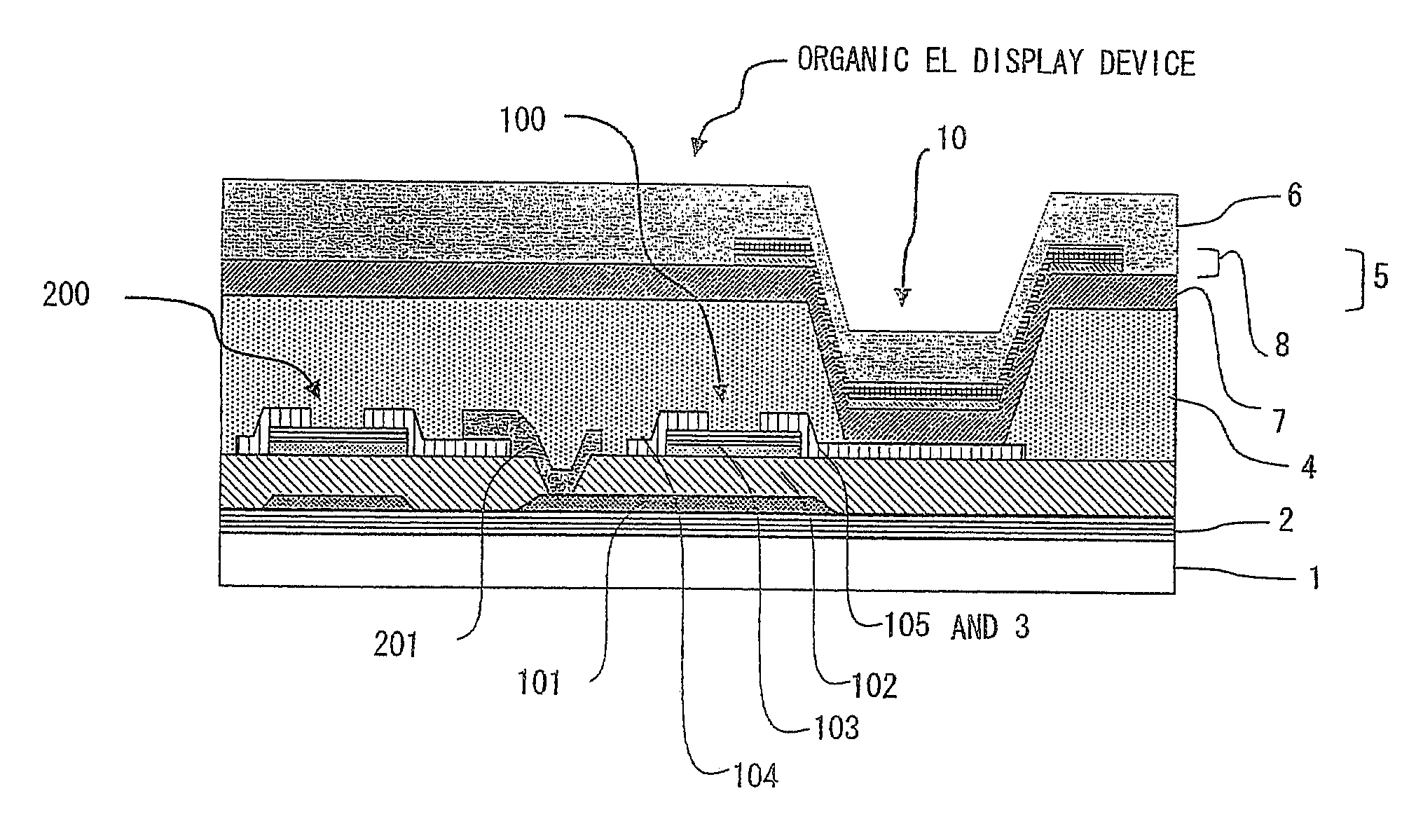
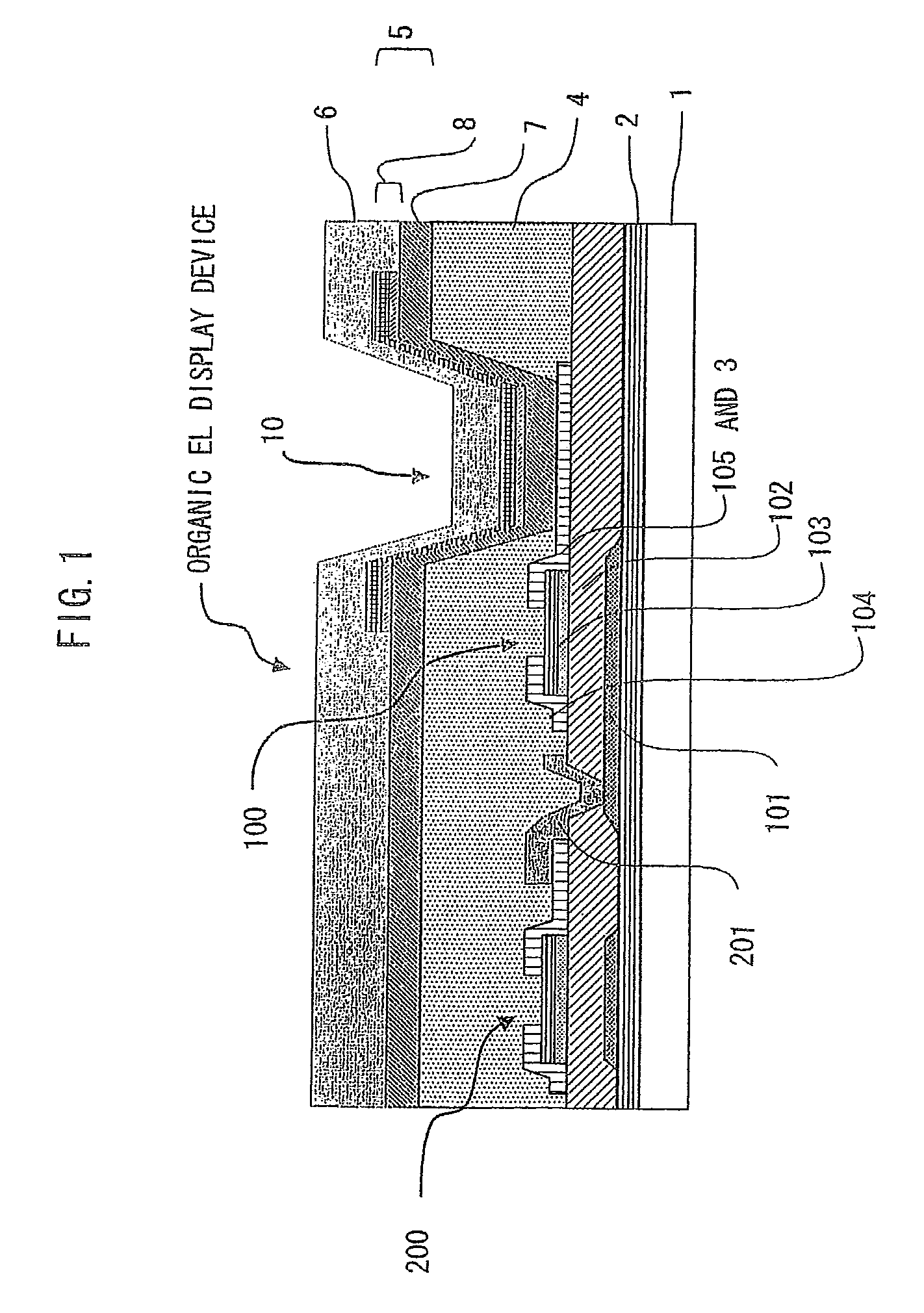
[0201]An organic EL display device 1 having a structure shown in FIG. 1 was produced.
1) Formation of Substrate Insulating Film
[0202]On a 5 inch×5 inch film of polyethylene naphthalate (simply referred to as PEN), SiON was deposited to a thickness of 500 nm by sputtering, thereby forming a substrate insulating film.
[0203]Sputtering condition: Sputtering was conducted by using an RF magnetron sputtering apparatus at an RF power of 400 W and a sputtering gas flow rate of Ar / O2=12.0 / 3.0 sccm. The target was Si3N4.
2) Formation of Gate Electrode (and Scanning Electric Wires)
[0204]After the substrate was washed, Mo was deposited to a thickness of 100 nm by sputtering. Then a photoresist was applied, a photomask was superposed thereon, and the photoresist was exposed through the photomask. Unexposed portions were cured by heating, and uncured photoresist was removed by a subsequent treatment with an alkaline developer. Thereafter treatment with an e...
example 2
[0263]An organic EL display device 2 was prepared in the same manner as in Example 1, except that the TFT was changed to a top-gate type TFT shown in FIG. 5.
[0264]The organic EL display device 2 was evaluated in the same manner as in Example 1, and it was found that an excellent emission surface state was obtained without emission unevenness, as in Example 1.
PUM
 Abstract
Description
Claims
Application Information