Unlock instant, AI-driven research and patent intelligence for your innovation.

Radiation detection system using solid-state detector devices

a detector device and detection system technology, applied in the field of radioation sensing and detection systems, can solve the problems of limited detection efficiency, high manufacturing cost, and inability to meet the needs of users, and achieve the effect of increasing length and increasing thickness

Inactive Publication Date: 2010-04-01
INNOVATIVE AMERICAN TECH
View PDF72 Cites 12 Cited by
  • Summary
  • Abstract
  • Description
  • Claims
  • Application Information

AI Technical Summary

Benefits of technology

[0006]Also, an embodiment of the present invention benefits from mass manufacturing techniques typically used in semiconductor manufacturing processes thereby yielding more cost effective neutron detection devices and systems. This enhances the commercial viability of a radiation and neutron detection system. Neutron detectors, according to the present invention, are built more rugged for more reliable use in many difficult operating conditions and rugged environments, while allowing remote monitoring by remotely located information processing systems and supervisory personnel.
[0012]Optionally, a neutron reactive coating layer, including a mixture of neutron reactive material such as Boron-10 and a polymer base vehicle, is disposed on the front contact layer and covering the openings of the plurality of filled elongated tube cavities thereby securely packing the neutron reactive material filling the plurality of elongated tube cavities.

Problems solved by technology

Past attempts at providing radiation and neutron detection systems have resulted in detection systems with limited sensitivity and efficiency at detecting, in particular, neutron radiation.
Further, these conventional implementations were very expensive to manufacture and fragile during use.
These characteristics of past neutron detectors detrimentally affected the commercial viability of radiation detection systems and particularly reduced their effectiveness in rugged-use environments.

Method used


Image

  • Radiation detection system using solid-state detector devices
  • Radiation detection system using solid-state detector devices
  • Radiation detection system using solid-state detector devices

Examples


Embodiment Construction

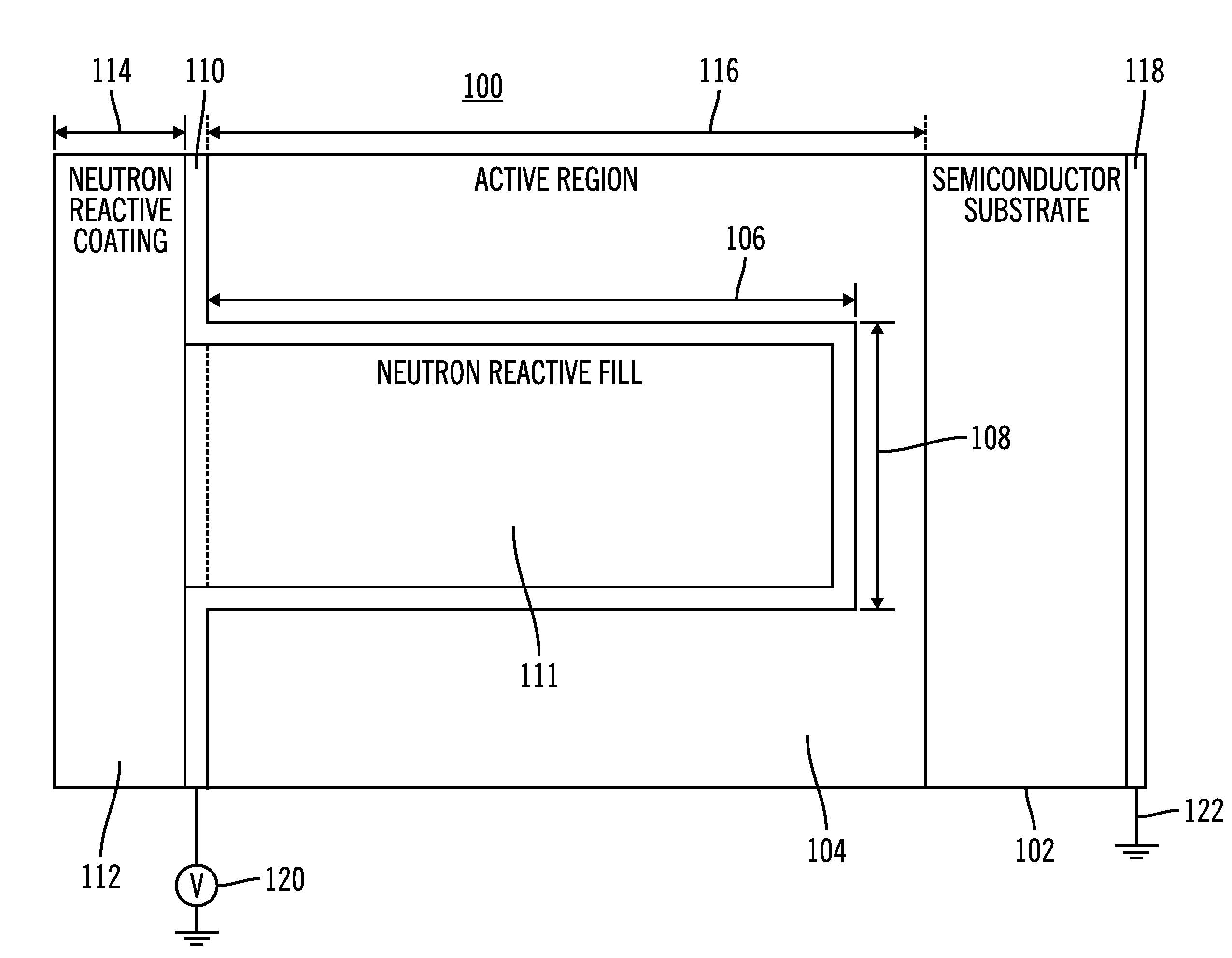
[0023]As required, detailed embodiments of the present invention are disclosed herein; however, it is to be understood that the disclosed embodiments are merely examples of the invention, which can be embodied in various forms. Therefore, specific structural and functional details disclosed herein are not to be interpreted as limiting, but merely as a basis for the claims and as a representative basis for teaching one skilled in the art to variously employ the present invention in virtually any appropriately detailed structure and function. Further, the terms and phrases used herein are not intended to be limiting; but rather, to provide an understandable description of the invention.

[0024]The terms “a” or “an”, as used herein, are defined as one or more than one. The term plurality, as used herein, is defined as two or more than two. The term another, as used herein, is defined as at least a second or more. The terms including and / or having, as used herein, are defined as comprisin...


PUM


Abstract

A neutron detection device (100) includes a semiconductor substrate including a gallium arsenide substrate region (102) having a back surface, and a high purity gallium arsenide active region (104) having a front surface. A back contact layer (118) is disposed on the back surface for providing a first voltage potential at the back surface. Elongated tube cavities extend from respective openings in the front surface into the active region (104) and almost through, but not totally through, the active region. A front contact layer is disposed on the front surface for providing a second voltage potential at the front surface. Neutron reactive material, e.g., pulverized Boron-10 powder, fills the elongated tube cavities to a high packing density. Optionally, spherical holes are formed into the substrate. The spherical holes are filled with neutron reactive material to enhance the efficiency of the neutron detection device.

Description

CROSS-REFERENCE TO RELATED APPLICATIONS[0001]This application is a continuation-in-part of prior co-pending U.S. patent application Ser. No. 11 / 291,574, filed on Dec. 1, 2005, now U.S. Pat. No. 7,592,601, and which was a continuation-in-part of U.S. patent application Ser. No. 10 / 280,255, filed on Oct. 25, 2002, which was based on prior U.S. Provisional Patent Application No. 60 / 347,997, filed on Oct. 26, 2001, and which further claimed priority from prior co-pending U.S. Provisional Patent Application No. 60 / 631,865, filed on Dec. 1, 2004; the entire collective teachings thereof being herein incorporated by reference.FIELD OF THE INVENTION[0002]The present invention generally relates to the field of radiation sensing and detection systems, and more particularly to a neutron detection system that uses solid-state or semiconductor neutron detectors.BACKGROUND OF THE INVENTION[0003]Past attempts at providing radiation and neutron detection systems have resulted in detection systems wi...

Claims


Application Information

Patent Timeline
IPC IPC(8): G01T3/08
CPCG01T3/08
Inventor FRANK, DAVID L.
Owner INNOVATIVE AMERICAN TECH
Features
  • R&D
  • Intellectual Property
  • Life Sciences
  • Materials
  • Tech Scout
  • Unparalleled Data Quality
  • Higher Quality Content
  • 60% Fewer Hallucinations
Learn More