
Method of producing a mixed substrate

a technology of mixed substrates and mixed substrates, which is applied in the direction of basic electric elements, semiconductor/solid-state device manufacturing, electrical equipment, etc., can solve the problems of partial consumption of silicon nitride, non-homogeneous substrate technology, and partial consumption of mixed substrates. achieve the effect of reducing surface roughness and effectively plane all projections

Inactive Publication Date: 2010-04-01
COMMISSARIAT A LENERGIE ATOMIQUE ET AUX ENERGIES ALTERNATIVES
View PDF11 Cites 2 Cited by
  • Summary
  • Abstract
  • Description
  • Claims
  • Application Information

AI Technical Summary

Benefits of technology

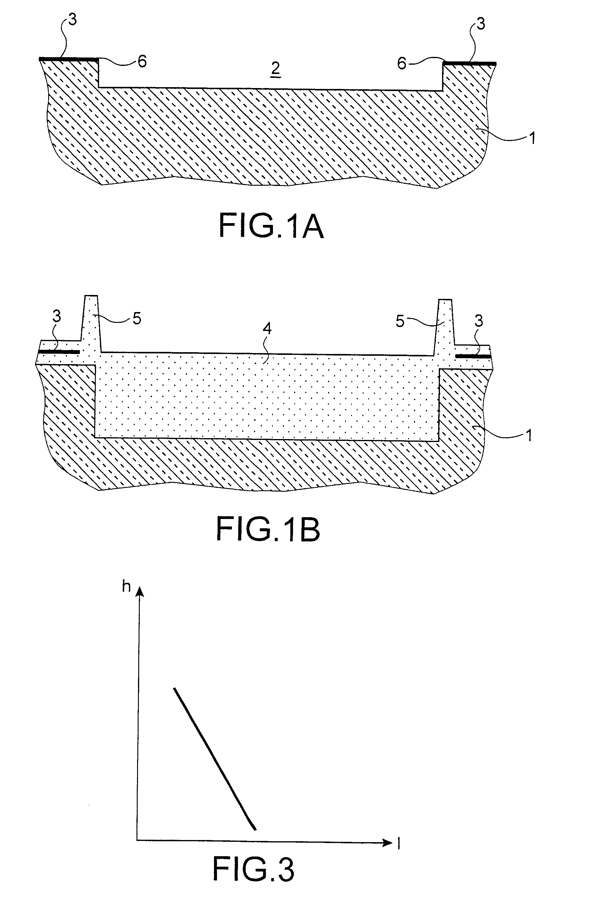
[0013]The present invention proposes a method of producing a mixed substrate in which the cavities are formed with regularly spaced projections, greatly reducing the surface roughness. The density and lateral dimensions of the projection are limited so as to be able to effectively plane all the projections by removing a minimum of surface material on the structured substrate. The distance separating the projections may be around a hundred micrometres and the width of the projections may be around 0.1 to 6 μm.

Problems solved by technology

However, the application of this technique to substrates having a non-homogeneous face may pose a problem.
The surface preparation of a mixed substrate with a view to its molecular bonding may pose a problem.
This is due to the oxidation process, which causes the partial consumption of the silicon nitride during the reaction.
One problem often encountered is that of a different efficacy of this planarization on the surfaces treated: this difference in efficacy depends for example on the distribution of the topologies on the surface or for example also to the nature of the different materials of the surface (selectivity of attack during mechanochemical planing).
This results in slight depressions on the surface.
It will be understood that these depressions are detrimental to close contact with a flat face of another substrate and that they give rise to bonding defects.
In addition, after assembly of the two substrates, if these depressions appear on electrically insulating areas of one of the substrates, the result may be a degradation of the dielectric integrity of the insulating areas.
Where it is wished for insulating areas of large size (several mm2, or even several cm2), attempts at topology planing are a failure since a surface hollowing is caused between the protrusions because of the large dimensions of the blocks to be obtained.
The result is flatness defects caused that prevent subsequent bonding, even if the surface roughness over dimensions of around a micrometre is satisfactory.
However, the electrical insulation may be defective vertically.

Method used


Image

  • Method of producing a mixed substrate
  • Method of producing a mixed substrate
  • Method of producing a mixed substrate

Examples


example application 1

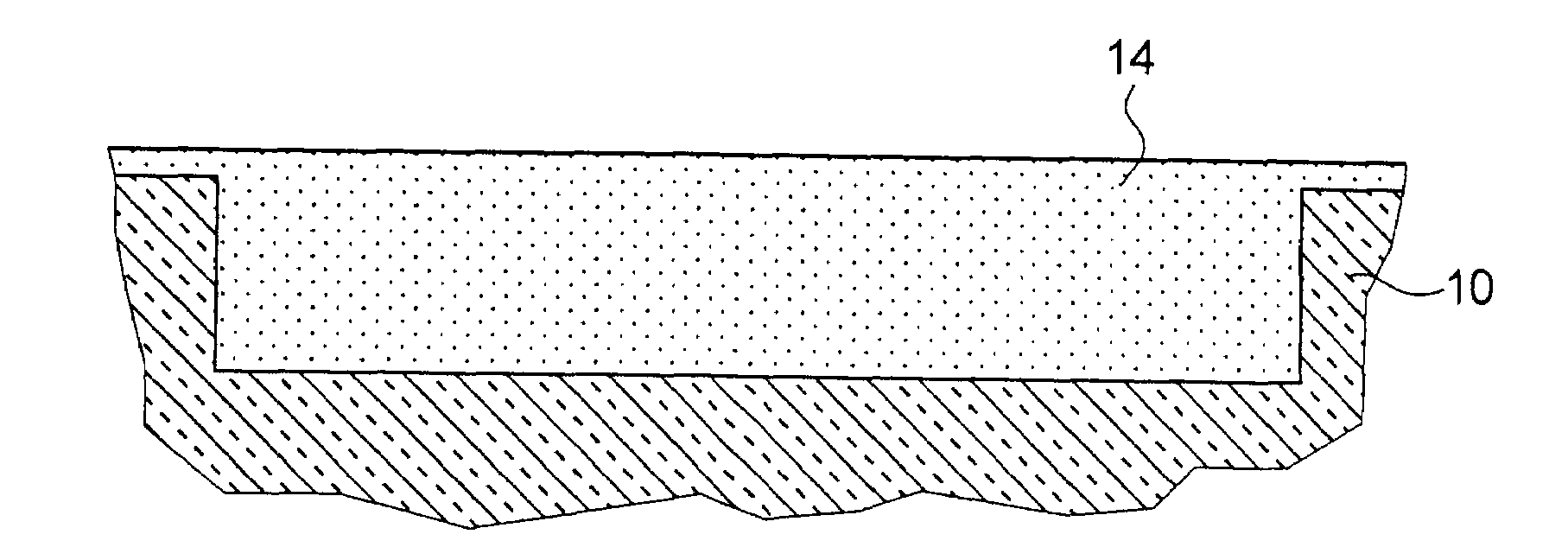
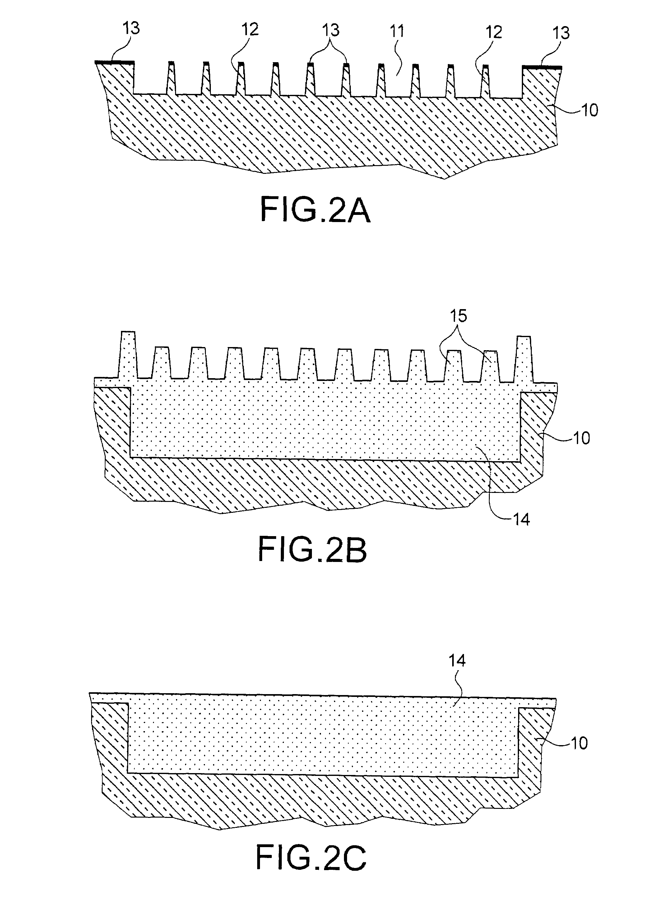
[0040]On the surface of a silicon substrate, a cavity is etched. This cavity, referenced 11 in FIG. 2A, consists of a set of sub-cavities or alveoli separated by parts or partitions or walls (referenced 12 in FIG. 2A) rising from the bottom of the cavity. The cavity has a depth of 1.5 μm. The alveoli have a width of 100 μm. The separation partitions or walls of the alveoli are 2 μm thick.

[0041]3 μm of silicon dioxide is produced at the etched area, by thermal oxidation at 1100° C. under steam. The area of the substrate situated outside the future insulating block is protected by a film of silicon nitride in order to prevent its oxidation. It will then be observed that the separation walls of the alveoli are oxidised over a height depending on the initial width of these walls and the thickness of oxide generated. Advantageously, the dimensions of these walls (and in particular the thickness) will be chosen so that the walls are oxidised over their entire initial height. Protrusions 0...

example application 2

[0044]On the surface of a silicon substrate, a cavity is etched. This cavity (referenced 11 in FIG. 2A) consists of a set of sub-cavities or alveoli separated by parts or partitions or walls (referenced 12 in FIG. 2A) rising from the bottom of the cavity. The cavity has a depth of 1.5 μm. The alveoli have a width of 100 μm. The separation partitions or walls of the alveoli are 4 μm thick.

[0045]3 μm of silicon dioxide is produced in the etched area, by thermal oxidation at 1100° C. under steam. The area of the substrate situated outside the future insulating block is protected by a film of silicon nitride in order to prevent its oxidation. It will then be observed that the alveoli separation walls are completely oxidised over a height of 0.5 μm. Protrusions 0.7 μm high will also be observed vertically in line with these walls. At the edge of the cavity, the protrusions have a height of between 1 μm and 1.2 μm.

[0046]After polishing and surface preparation, this substrate can be assemb...

example application 3

[0047]On the surface of a silicon substrate, a cavity is etched. This cavity consists of a set of alveoli separated by walls or spacers rising from the bottom of the cavity. The cavity has a depth of 1.5 μm. The alveoli have a width of 100 μm. The alveoli separation walls are 2 μm thick.

[0048]The area situated outside the future insulating block is therefore covered with a film of silicon oxide obtained for example thermally, chemically or by dry method of the plasma or UV / O3 type, referred to as a pedestal film. The thickness of this film is less than 0.5 μm, preferably less than 50 nm and preferably again less than 20 nm. This film of oxide is protected by a film of silicon nitride intended to form a barrier to subsequent oxidation.

[0049]3 μm of silicon oxide is produced in the etched area, by thermal oxidation at 1100° C. under steam. It is then observed that the alveoli separation walls are completely oxidised over a height of 2 μm. Protrusions 0.8 μm high are also observed vert...


PUM

PropertyMeasurementUnit
widthaaaaaaaaaa
widthaaaaaaaaaa
widthaaaaaaaaaa

Abstract

The invention concerns a method of producing a mixed substrate, that is to say a substrate comprising at least one block of material different from the material of the substrate, the method comprising the following successive steps:formation of a cavity in a substrate of first material, and from one of its faces, the formation of the cavity being carried out so as to leave at least part of the first material projecting from the bottom of the cavity,formation of the block by means of a reaction, initiated from the walls of the cavity, between the first material and at least one chemical element contributed in order to obtain a second material filling the cavity, the formation of the block being carried out so as to obtain, from the part of the first material projecting, a protrusion of second material projecting on said face of the substrate.

Description

TECHNICAL FIELD[0001]The invention relates to a method of producing a mixed substrate intended for manufacturing specific stacked structures. Such a stacked structure is obtained by bonding the mixed substrate with another substrate or a layer on a bonding interface.PRIOR ART[0002]It is often necessary, in the semiconductor field, to manufacture structures by stacking and bonding. For example, two substrates may be assembled by molecular bonding (or “wafer bonding”) of a main face of one of the substrates with a main face of the other substrate. For this purpose, the faces to be put in contact must be carefully prepared to allow this molecular bonding. This preparation may involve chemical-mechanical polishing of the faces to be put in contact, cleaning of these faces and activation thereof in order to obtain close contact (faces of mirror quality).[0003]This molecular bonding technique procures very good results for the bonding of semiconductor substrates having faces that are homo...

Claims


Application Information

Patent Timeline
Patent Type & Authority Applications(United States)
IPC IPC(8): H01L21/306
CPCH01L21/31053H01L21/76251H01L21/76208
Inventor MORICEAU, HUBERTSATORI, SYLVIECHARVET, ANNE-MARIE
Owner COMMISSARIAT A LENERGIE ATOMIQUE ET AUX ENERGIES ALTERNATIVES
Learn More