Imaging device with sense and couple electrodes

a technology of sensing device and electrode, which is applied in the direction of solid-state devices, instruments, material analysis, etc., can solve the problems of reducing sensing sensitivity, and achieve the effect of increasing the thickness of the protection insulating layer without reducing sensing sensitivity

Active Publication Date: 2010-04-08
EGIS TECH
View PDF2 Cites 42 Cited by
  • Summary
  • Abstract
  • Description
  • Claims
  • Application Information

AI Technical Summary

Benefits of technology

[0009]It is therefore an object of the invention to provide an imaging device capable of effectively increasing the thickness of the protection insulating layer without decreasing the sensing sensitivity.

Problems solved by technology

However, the too-thick protection layer causes the very small sense capacitance (C_cell) and thus decreases the sensing sensitivity.

Method used


Image

  • Imaging device with sense and couple electrodes
  • Imaging device with sense and couple electrodes
  • Imaging device with sense and couple electrodes

Examples


first embodiment

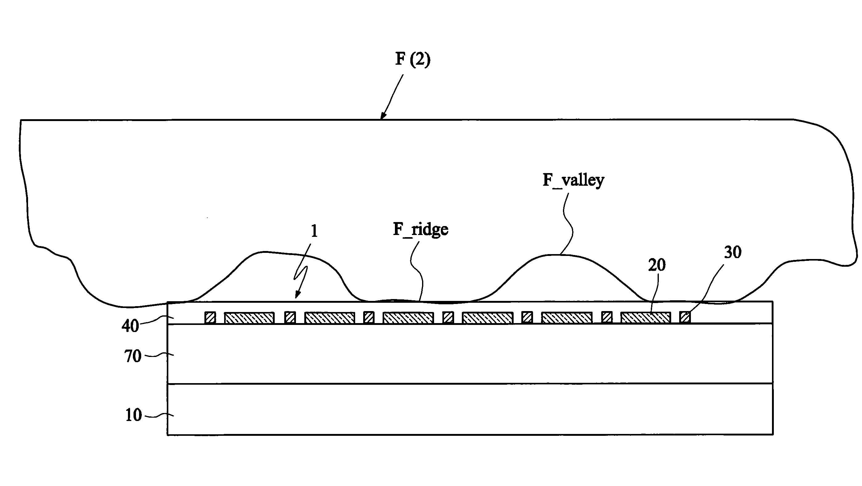
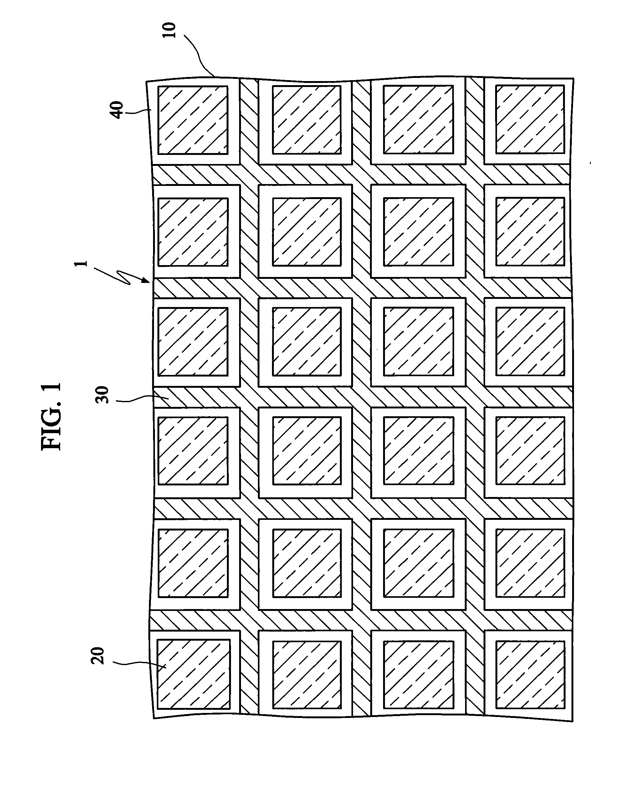
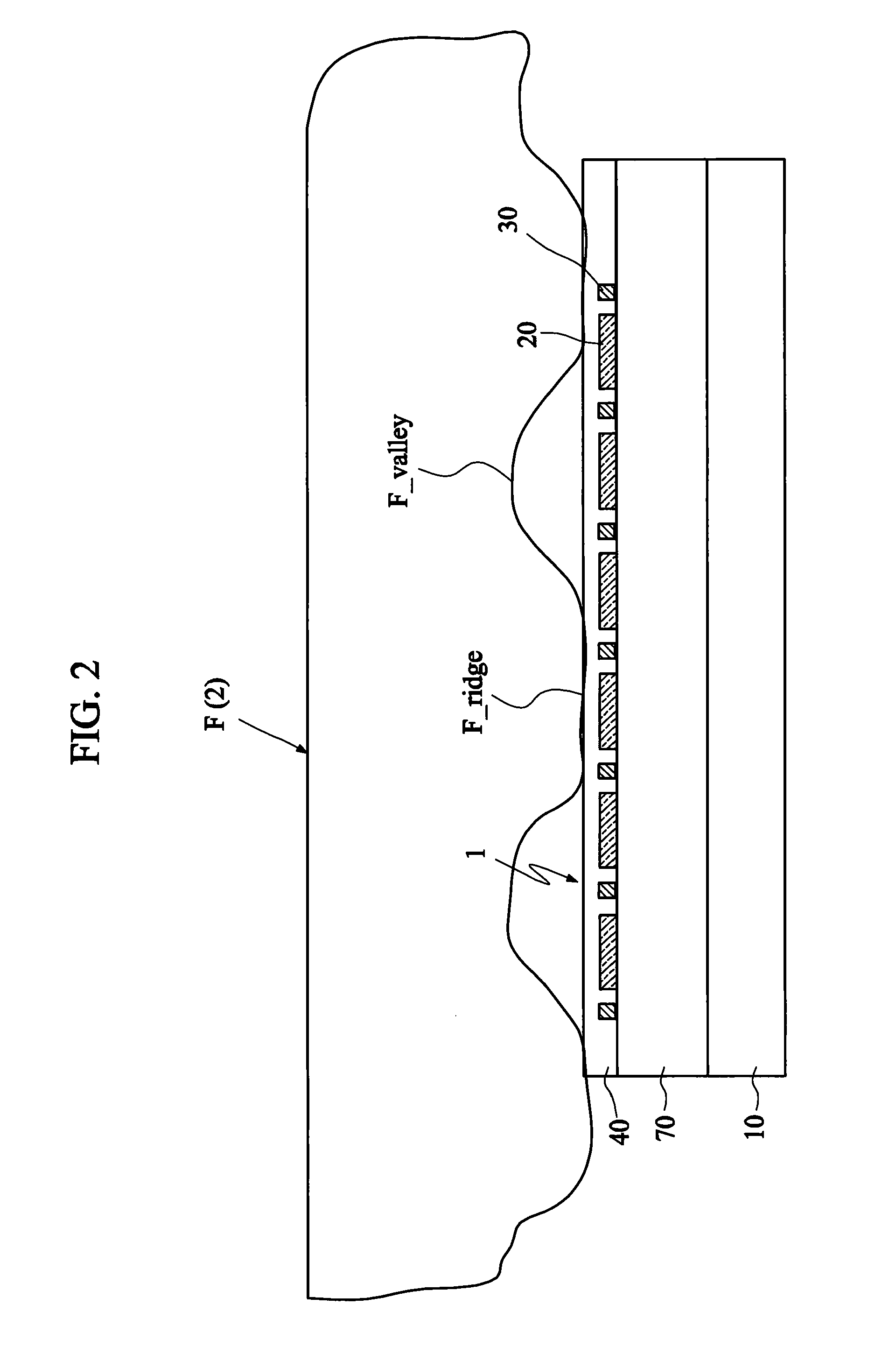
[0026]FIG. 1 is a schematic top view showing a portion of a sensing member array of an imaging device 1 of the invention. FIG. 2 is a schematic illustration showing the imaging device of the invention in a used state. FIG. 3 is a schematic illustration showing an enlarged cross-section of a single sensing member according to the invention. Referring to FIGS. 1 to 3, the imaging device 1 of this embodiment is for sensing an image of an object 2. The imaging device 1 includes at least a negative feedback amplifier 12, a substrate 10, a sense electrode 20, a couple electrode 30 and an insulation protection layer 40.

[0027]The material of the substrate 10 in this invention may be a silicon material, a glass material, other semiconductor materials or other insulation materials or polymer materials. The imaging device includes a sensing member array, composed of sensing members, to be in contact with a skin texture, and further includes a sense circuit, an amplifier circuit, an analog-to-d...

second embodiment

[0048]FIG. 6 is a schematic illustration showing an enlarged cross-section of a single sensing member according to the invention. Referring to FIG. 6, the imaging device 1 further includes a driving voltage generator 50 for generating a driving voltage V_drive, which is in direct contact with or coupled to the object 2. The human body is a charged body, and the sensitivity variation during measurement is increased due to different electric properties of different persons. Thus, the potential control may be provided when the imaging device is touched by the skin. As shown in FIG. 6, it is possible to connect the driving voltage V_drive to the skin. The driving voltage V_drive may be provided by the method including, without limitation to, providing a conductor (not shown) to be touched by the skin. Alternatively, a couple capacitor, a resistor or an inductor may be connected between the conductor and the skin to couple the DC or AC signal to the skin to provide the driving voltage V_...


PUM


Abstract

An imaging device for sensing an image of an object includes a negative feedback amplifier, a substrate, a sense electrode, a couple electrode and an insulation protection layer. The sense and couple electrodes are disposed above the substrate. The insulation protection layer covers the sense and couple electrodes. The sense electrode and the object form a sense capacitor. The couple electrode and the object form a couple capacitor. A negative input terminal of the negative feedback amplifier is electrically connected to the sense electrode, and the couple electrode is electrically connected to a signal output terminal of the negative feedback amplifier and a signal input terminal of the imaging device.

Description

[0001]This application claims priority of No. 097138647 filed in Taiwan R.O.C. on Oct. 8, 2008 and priority of No. 098109837 filed in Taiwan R.O.C. on Mar. 26, 2009 under 35 USC 119, the entire content of which is hereby incorporated by reference.BACKGROUND OF THE INVENTION[0002]1. Field of the Invention[0003]The invention relates in general to an imaging device, and more particularly to an imaging device for sensing skin textures.[0004]2. Related Art[0005]In the technology of sensing the capacitor of the skin of the human body, a fingerprint sensor for sensing the texture of the finger or a touch panel or a touch screen for capacitor touch control may be applied.[0006]More particularly, the sensor for sensing the texture of the skin has a portion for contacting the texture of the skin, and the basic structure of the portion includes an array-type sensing member. That is, several sensing members having the same structure constitute a two-dimensional sensor array. For example, when t...

Claims


Application Information

Patent Timeline
Patent Type & Authority Applications(United States)
IPC IPC(8): H03F3/08H01L31/02G06V30/144
CPCH03F3/08H01L27/14678
Inventor CHOU, BRUCE C.S.
Owner EGIS TECH
Why Eureka
Try Eureka