
Method for structuring silicon carbide with the aid of fluorine-containing compounds

a technology of silicon carbide and fluorine, which is applied in the direction of decorative surface effects, electrical equipment, decorative arts, etc., can solve the problems of high equipment complexity and the need to generate gas plasma for etching sic, and achieve the effect of further adjusting the selectivity of the etching process

Inactive Publication Date: 2010-04-08
ROBERT BOSCH GMBH
View PDF5 Cites 13 Cited by
  • Summary
  • Abstract
  • Description
  • Claims
  • Application Information

AI Technical Summary

Benefits of technology

[0010]Using the method according to the present invention, etching rates in SiC from ≧1 μm / min to ≦20 μm / min are achieved, depending on the procedure. It is advantageous in the method according to the present invention in particular that it runs free of plasma, i.e., no etching gas plasma needs to be used.

Problems solved by technology

The advantage of stability due to its kinship with diamond is, however, also a challenge in structuring the SiC material.
The disadvantage here, however, is that a gas plasma must be generated for etching SiC.
This involves a high degree of equipment complexity.

Method used


Image

  • Method for structuring silicon carbide with the aid of fluorine-containing compounds
  • Method for structuring silicon carbide with the aid of fluorine-containing compounds
  • Method for structuring silicon carbide with the aid of fluorine-containing compounds

Examples


Embodiment Construction

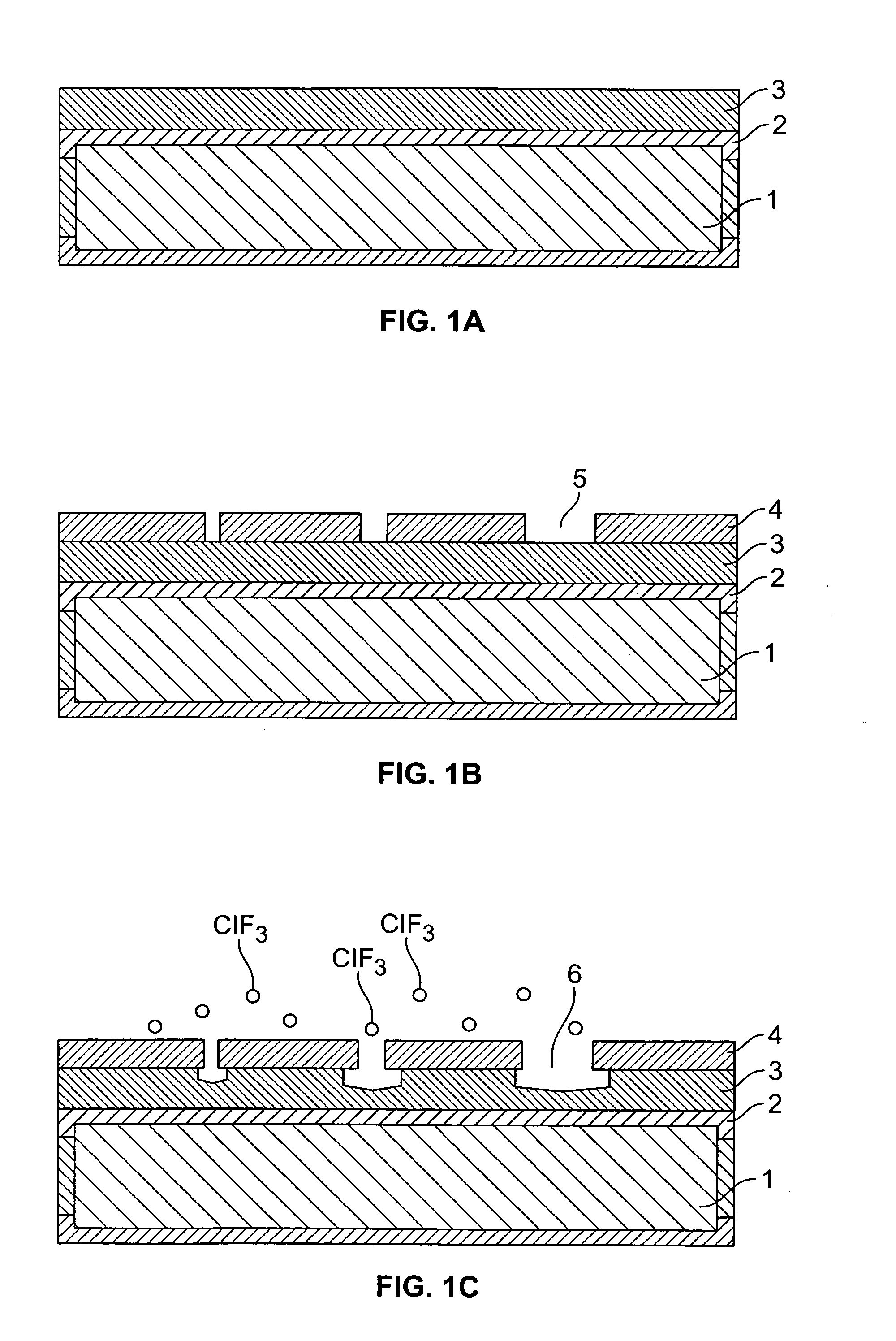
[0024]FIG. 1a shows the initial situation for a method according to the present invention. An Si3N4-layer 2 is initially situated on a wafer 1 having a layer substructure which is not shown in detail. An SiC layer 3 to be structured is situated on this nitride layer.

[0025]FIG. 1b shows the situation after an SiO2 layer 4 has been deposited on the SiC layer using a PECVD method. Subsequently the structures to be produced are represented on oxide layer 4 with the aid of a photolithography step (not shown). The masking layer and the PECVD oxide are structured with the aid of customary oxide structuring methods. Thus, accesses 5 are created for structuring SiC layer 3.

[0026]FIG. 1c shows the etching attack by ClF3 on SiC layer 3. The etching rate and the isotropy or anisotropy may be adjusted as appropriate via the selection of the process parameters. Here it is shown how etched-out areas 6 get underneath masking layer 4.

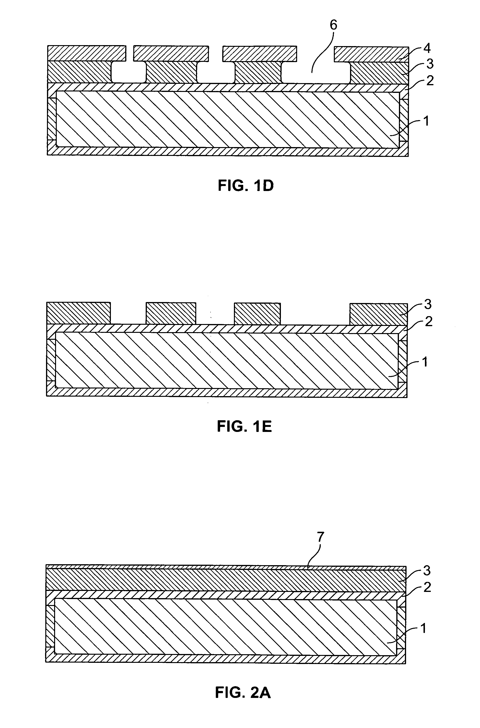
[0027]In FIG. 1d the etching of SiC layer 3 is completed. FIG. 1e ...


PUM

PropertyMeasurementUnit
Concentrationaaaaaaaaaa

Abstract

A method for etching silicon carbide, a mask being produced on a silicon carbide layer, the unmasked areas of the silicon carbide layer being etched using a fluorine-containing compound, which is selected from the group including interhalogen compounds of fluorine and / or xenon difluoride. The use of chlorine trifluoride, chlorine pentafluoride, and / or xenon difluoride for structuring silicon carbide layers covered with masks containing silicon dioxide and / or silicon oxide carbide; a structured silicon carbide layer obtained by the method, and a microstructured electromechanical component or a microelectronic component including a structured silicon carbide layer obtained by the method.

Description

FIELD OF THE INVENTION[0001]The present invention relates to a method for etching silicon carbide, a mask being produced on a silicon carbide layer. It furthermore relates to the use of chlorine trifluoride, chlorine pentafluoride, and / or xenon difluoride for structuring silicon carbide layers covered with masks containing silicon dioxide and / or silicon oxide carbide, a structured silicon carbide layer obtained by the method according to the present invention, and a microstructured electromechanical component or a microelectronic component including a structured silicon carbide layer obtained by the method according to the present invention.BACKGROUND INFORMATION[0002]Silicon carbide (SiC) is, by its structure and properties, similar to diamond, since silicon and carbon are located in the same main group and adjacent periods of the periodic system and their atomic diameters are of a similar order of magnitude. The advantage of stability due to its kinship with diamond is, however, a...

Claims


Application Information

Patent Timeline
IPC IPC(8): C01B31/36B44C1/22
CPCC04B41/5346C04B41/91H01L21/3081H01L21/3065C04B2111/00844
Inventor RUDHARD, JOACHIMFUCHS, TINO
Owner ROBERT BOSCH GMBH
Learn More