Solid-state imaging device and signal processing system

a solid-state imaging and signal processing technology, applied in the field of solid-state imaging devices and signal processing systems, can solve the problems of heat due to positional relationship between solid-state imaging devices and light emitting elements that have not been solved, and the heat provided to solid-state imaging devices has not been solved, so as to improve flexibility regarding the layout of optical communication units, improve flexibility regarding the layout of cooling units for optical communication units, and improve the effect of flexibility

Inactive Publication Date: 2010-04-15
SONY CORP
View PDF16 Cites 11 Cited by
  • Summary
  • Abstract
  • Description
  • Claims
  • Application Information

AI Technical Summary

Benefits of technology

[0015]Also, flexibility regarding the layout of the optical communication unit improves, whereby flexibility regarding the layout of the cooling units for the optical communication units also improves. Various types of cooling system can be employed, for example, such as a system wherein the optical communication units are disposed grouped, and are cooled in a batch, a system wherein the optical communication units are disposed discretely, and heat sources are cooled discretely, and so forth.
[0016]Further, flexibility regarding the layout of the optical communication units improves, whereby various types of signal transmission method can be empl

Problems solved by technology

However, with the technology described in Japanese Unexamined Patent Application Publication No. 2006-196972, only a configuration has been disclosed wherein light emitting elements are mounted on a substrate on which a solid-state imaging device has been mounted, and no description has been made regarding the layout of the light emitting elements.
Therefore, a problem regarding heat due to position

Method used


Image

  • Solid-state imaging device and signal processing system
  • Solid-state imaging device and signal processing system
  • Solid-state imaging device and signal processing system

Examples


first embodiment

Configuration Example of Solid-State Imaging Device

(1-1) Configuration Example of Solid-State Imaging Device in which Optical Communication Units are Disposed Grouped

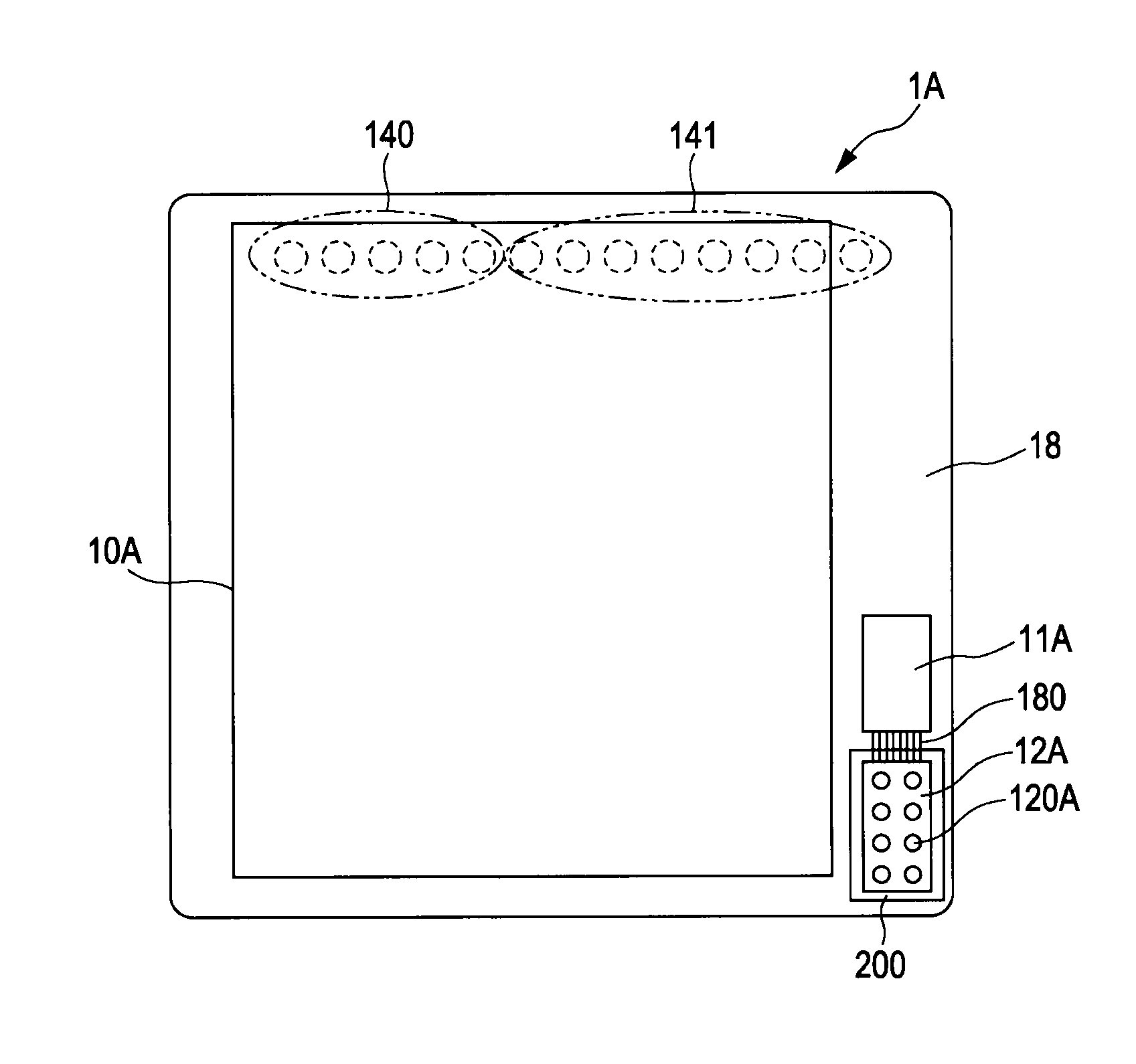
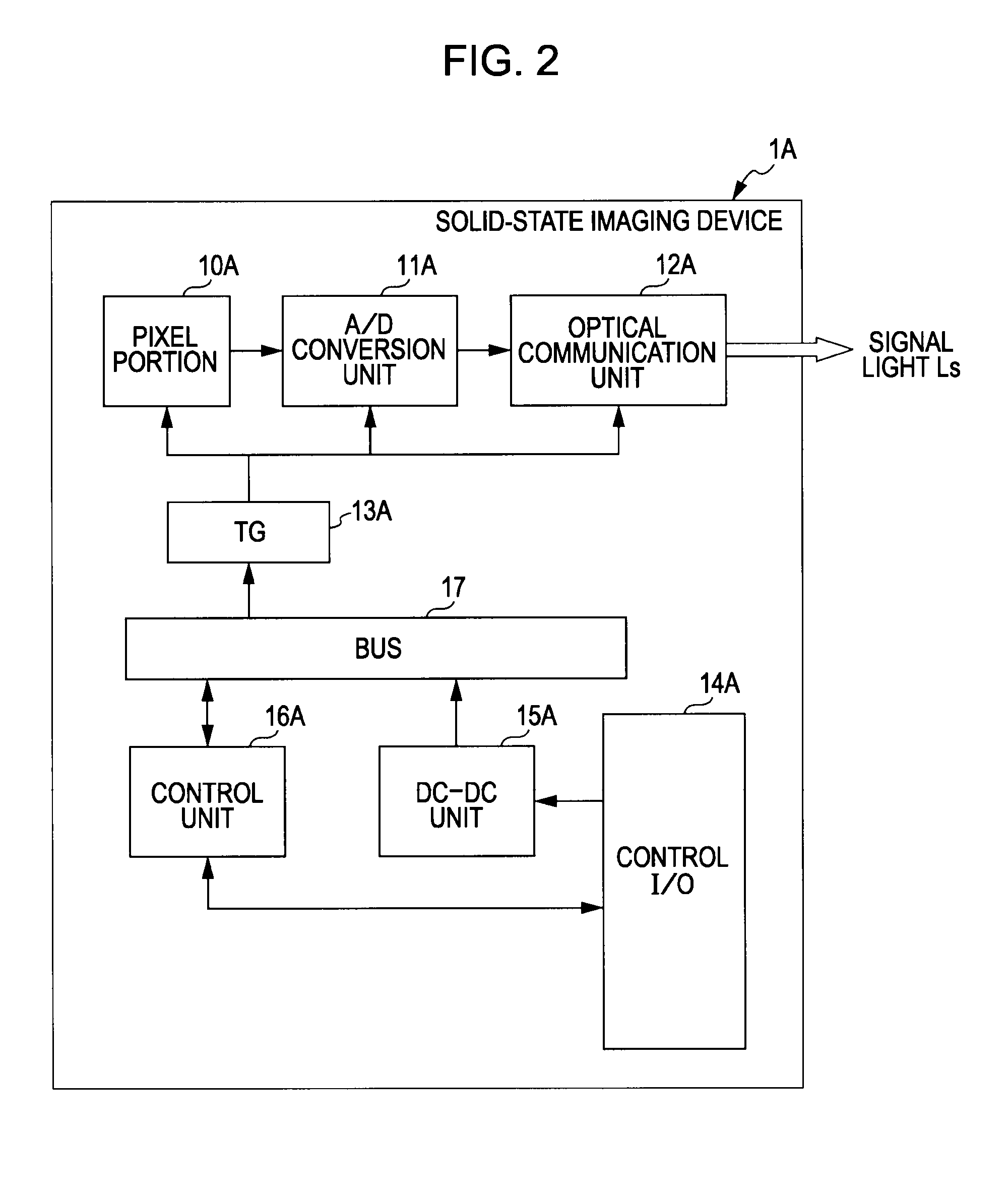
[0078]FIG. 1 is a schematic plan view illustrating an example of a solid-state imaging device in which optical communication units are disposed grouped. FIG. 2 is a functional block diagram illustrating an example of functions used for realizing the solid-state imaging device according to each of embodiments.

[0079]A solid-state imaging device 1A in which an optical communication unit is disposed grouped is configured of a CMOS (Complementary Metal Oxide Semiconductor) image sensor, or a CCD (Charge Coupled Device) image sensor. The solid-state imaging device 1A includes a pixel portion 10A which converts light into an electric signal to output this. With the pixel portion 10A, pixels which convert light into electricity are arrayed two-dimensionally or one-dimensionally, from which an electric signal according to the in...


PUM


Abstract

A solid-state imaging device includes: a pixel portion configured to convert light into an electric signal; a substrate where the pixel portion is formed; an A/D conversion unit configured to convert a signal read out from the pixel portion into a digital signal; and an optical communication unit configured to convert a signal digitized by the A/D conversion unit into an optical signal, and output the optical signal, with the single optical communication unit or a plurality of the optical communication units being disposed grouped in the vicinity portion of the substrate around the pixel portion.

Description

BACKGROUND OF THE INVENTION[0001]1. Field of the Invention[0002]The present invention relates to a solid-state imaging device which converts an optical image into an electric signal, and a signal processing system including this solid-state imaging device, and more specifically, relates to a solid-state imaging device which converts an optical image into an electric signal, and a signal processing system including this solid-state imaging device, whereby a pixel signal to be read out from the solid-state imaging device can be output as an optical signal.[0003]2. Description of the Related Art[0004]Increased speed and integration of circuit substrates has advanced, and accordingly, there is pressing demand for handling of problems such as signal delay, occurrence of EMI, and so forth. Optical wiring technology has attracted attention wherein signal delay, signal deterioration, and electromagnetic interference noise irradiated from wiring that have been problems due to electric wiring...

Claims


Application Information

Patent Timeline
IPC IPC(8): H04N5/335H04N5/225G03B17/02H04N5/378
CPCH04N5/2257H04N5/378H04N7/22H01L2924/0002H01L2924/00H04N23/57H04N25/75
Inventor OGASAWARA, HIDEHIKOSEKIYA, TOSHIYUKI
Owner SONY CORP
Why Eureka
Try Eureka