

Solid-state image sensor and camera system
a camera system and image sensor technology, applied in the field of solid-state image sensors, can solve the problems of noise and significant increase in system complexity, and achieve the effects of suppressing the increase in circuit area, reducing the noise of ad converters, and increasing frame ra
- Summary
- Abstract
- Description
- Claims
- Application Information
AI Technical Summary
Benefits of technology
Problems solved by technology
Method used
Image

Examples
Embodiment Construction
[0039]Hereinafter, embodiments of the present invention will be described in conjunction with the accompanying drawings. The description will proceed as follows.
[0040]1. Overall exemplary configuration of solid-state image sensor
[0041]2. Exemplary configuration of a comparator
[0042]3. CDS considerations
[0043]4. Comparator operation
[0044]5. Modification of comparator
[0045]6. Exemplary configuration of a camera system
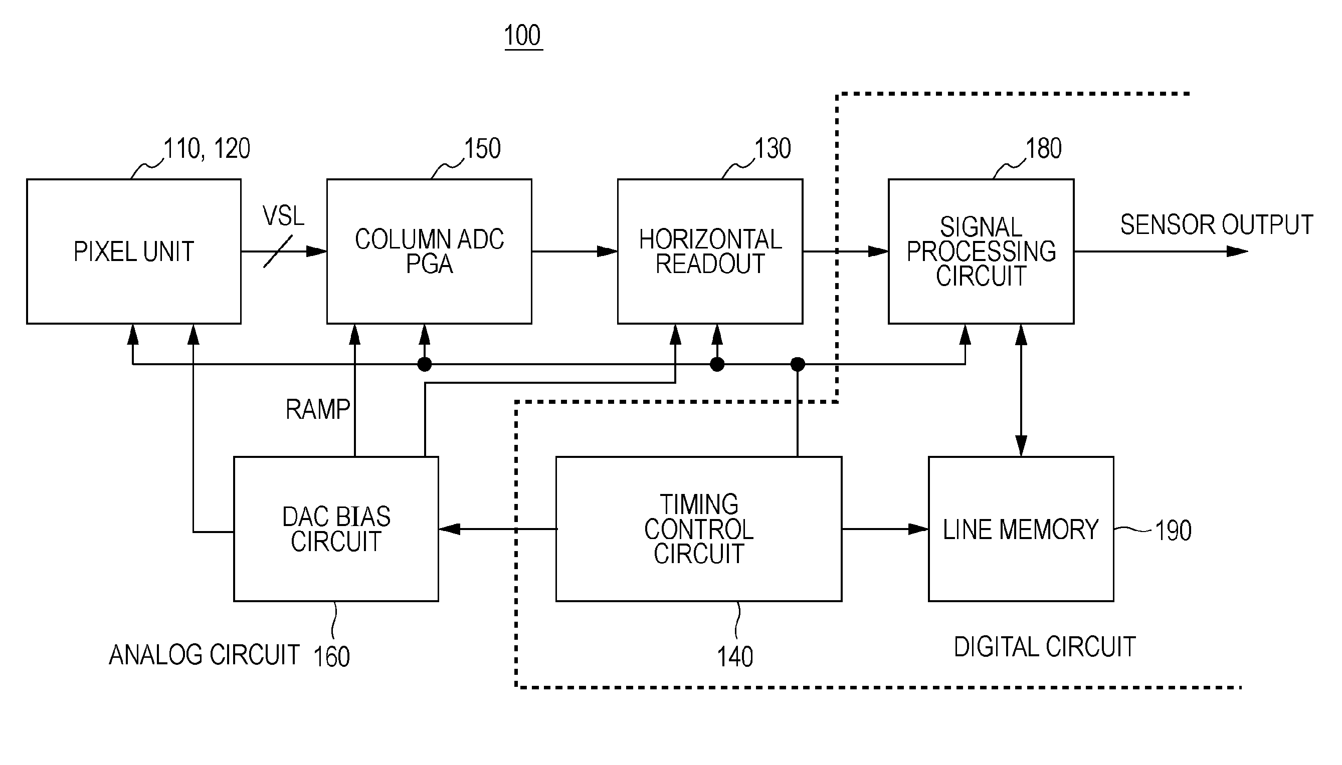
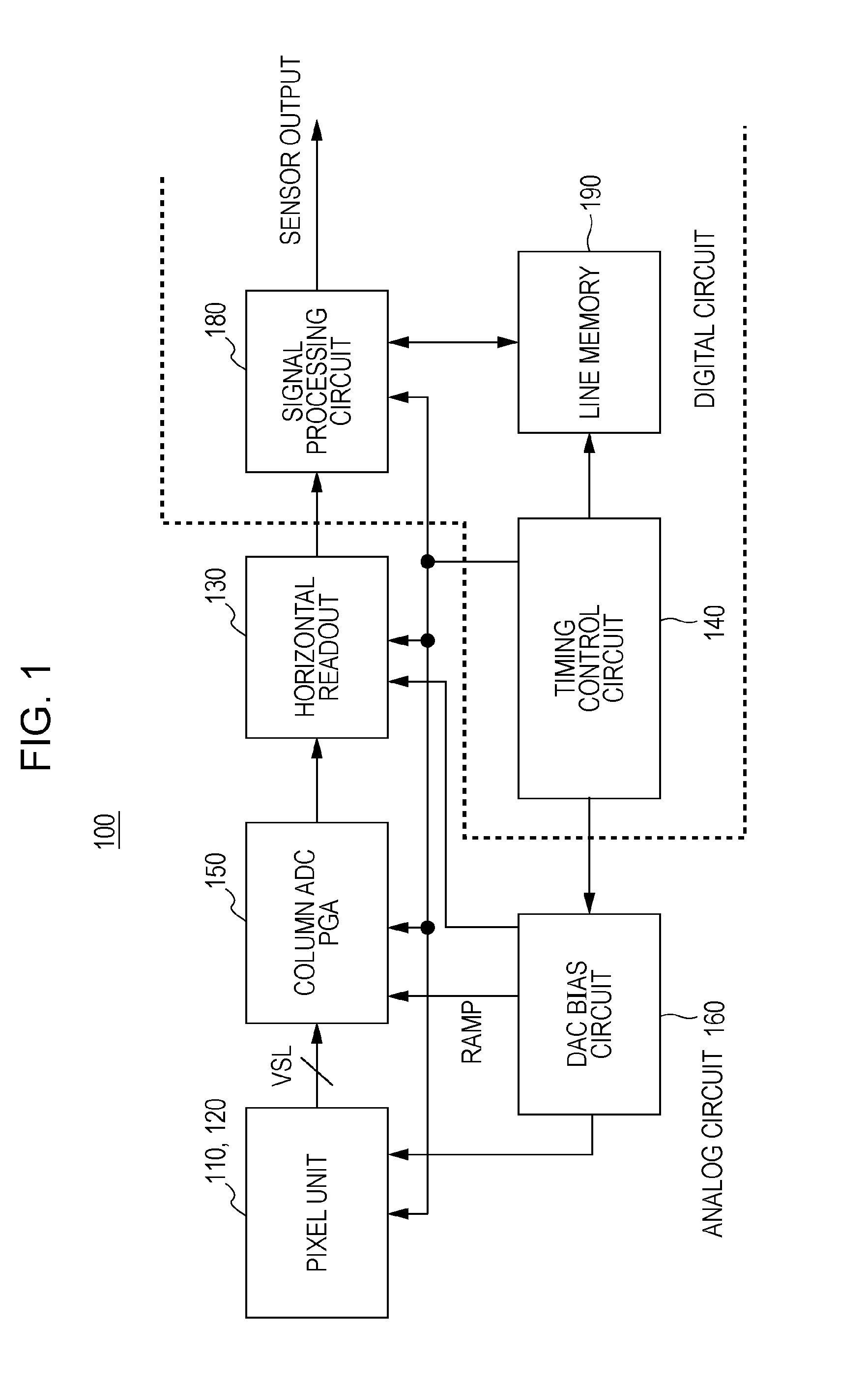
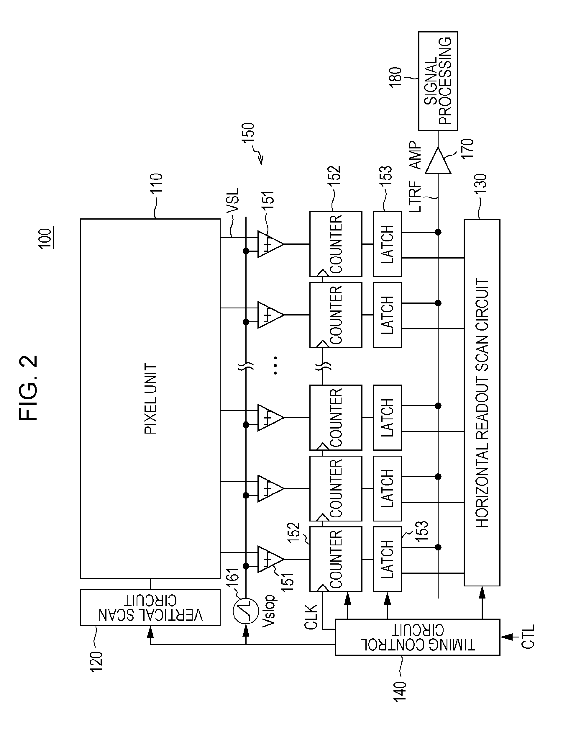
[0046]FIG. 1 is a block diagram illustrates an exemplary configuration of a column-parallel ADC solid-state image sensor (i.e., CMOS image sensor) in accordance with an embodiment of the present invention. FIG. 2 is a block diagram illustrating, in further detail, the ADC group in the column-parallel ADC solid-state sensor (i.e., CMOS image sensor) shown in FIG. 1.
[0047]As shown in FIGS. 1 and 2, the solid-state image sensor 100 includes a pixel unit 110, a vertical scan circuit 120, a horizontal readout scan circuit 130, and a timing generator circuit 140 that constitute...
PUM
 Abstract
Description
Claims
Application Information