Automated optimization of an integrated circuit layout using cost functions associated with circuit performance characteristics

a technology of cost function and integrated circuit, applied in multi-objective optimization, cad techniques, instruments, etc., can solve the problems of reducing manufacturing yield, complex integrated circuit design and semiconductor fabrication processes, and increasing challenges in semiconductor integrated circuit design and manufacturing processes, so as to reduce variability, improve performance, and reduce power consumption

Inactive Publication Date: 2010-04-22
MITTAL ANURAG
View PDF6 Cites 107 Cited by
  • Summary
  • Abstract
  • Description
  • Claims
  • Application Information

AI Technical Summary

Benefits of technology

[0022]Accordingly, one object of the present invention is to provide an optimization of a layout of an integrated circuit (IC) wherein an assessment is taken into account of the circuit performance characteristics of the associated layout. The circuit performance characteristics are a function of the circuit performance parameters such as the P-N transistor size ratio, power budget, chip frequency/timing, etc. Also, circuit performance parameters for a given layout can be a function of device parameters such as mobility, ION, etc., which can...

Problems solved by technology

Semiconductor integrated circuit (IC) design and manufacturing processes have become increasingly challenging with each new technology node.
Integrated circuit designs and semiconductor fabrication processes are extremely complex, since hundreds of processing steps may be involved.
Occurrence of variations or lack of process control at any of the process steps may necessitate redesign or cause lower manufacturing yield, where manufacturing yield may be defined as the number of functional chips produced as compared to the theoretical number of chips that could be produced.
In addition to manufacturing yield lo...

Method used


Image

  • Automated optimization of an integrated circuit layout using cost functions associated with circuit performance characteristics
  • Automated optimization of an integrated circuit layout using cost functions associated with circuit performance characteristics
  • Automated optimization of an integrated circuit layout using cost functions associated with circuit performance characteristics

Examples


Embodiment Construction

[0037]The present invention is particularly applicable to a computer-implemented software-based IC design system for generating an IC design using circuit performance characteristic optimization to manipulate an IC design layout, and it is in this context that the various embodiments of the present invention will be described. It will be appreciated, however, that the IC design system and method for providing circuit performance characteristic optimization in accordance with the various embodiments of the present invention have greater utility, since they may be implemented in hardware or may incorporate other modules or functionality not described herein.

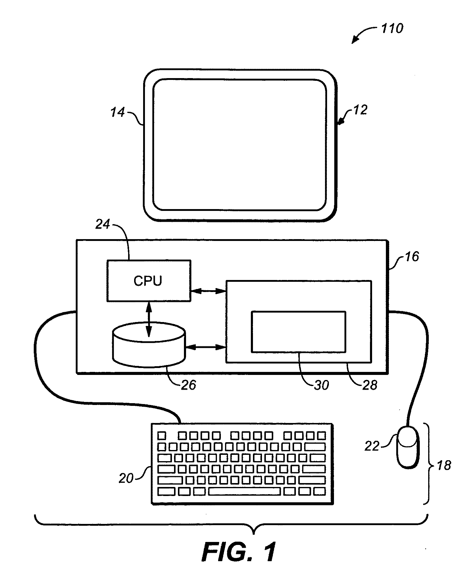
[0038]FIG. 1 is a block diagram illustrating an example of an IC design system 10 for providing circuit performance characteristic optimization in accordance with one embodiment of the present invention implemented on a personal computer 12. In particular, the personal computer 12 may include a display unit 14, which may be a catho...


PUM


Abstract

An integrated circuit (IC) design system and method provide an optimization of a layout of an integrated circuit wherein an assessment is taken into account of the circuit performance characteristics and the layout of the IC design. The system and method assess associated circuit performance characteristics, each as a cost function of a local pattern of shapes in an initial circuit layout, aggregate cost functions of the associated circuit performance characteristics to derive an integral performance number associated to the initial global circuit layout, perturb the integral performance number by varying the global circuit layout, and select perturbations that optimize the performance number, so as to optimize the global circuit layout. Assessment is taken into account of the circuit performance characteristics based on the layout and the interdependence of the circuit performance characteristics for the IC design. The physical process related effects such as well proximity effect and stress/strain engineering and/or performance parameters such as the P-N transistor size ratio are taken into account to achieve optimization.

Description

BACKGROUND OF THE INVENTION[0001]1. Field of the Invention[0002]The present invention relates generally to a system and method for designing integrated circuits or migrating integrated circuit designs from one technology node to another for fabrication by a semiconductor manufacturing process and, more particularly, to a system and method for optimizing an integrated circuit layout. Specifically, various embodiments of the present invention provide a system and method to optimize the integrated circuit layout based on associated circuit performance characteristics.[0003]2. Description of the Prior Art[0004]Semiconductor designs and fabrication processes are continually evolving and the semiconductor manufacturing industry is continually developing new processes to produce smaller and smaller geometries of the designs being manufactured, because semiconductor devices typically consume less power and operate at higher speeds as they scale to smaller dimensions. Semiconductor integrate...

Claims


Application Information

Patent Timeline
IPC IPC(8): G06F17/50
CPCG06F17/5036G06F2217/08G06F17/5068G06F30/367G06F30/39G06F2111/06
Inventor MITTAL, ANURAG
Owner MITTAL ANURAG
Why Eureka
Try Eureka