Structural member having a plurality of conductive regions
- Summary
- Abstract
- Description
- Claims
- Application Information
AI Technical Summary
Benefits of technology
Problems solved by technology
Method used
Image
Examples
first embodiment
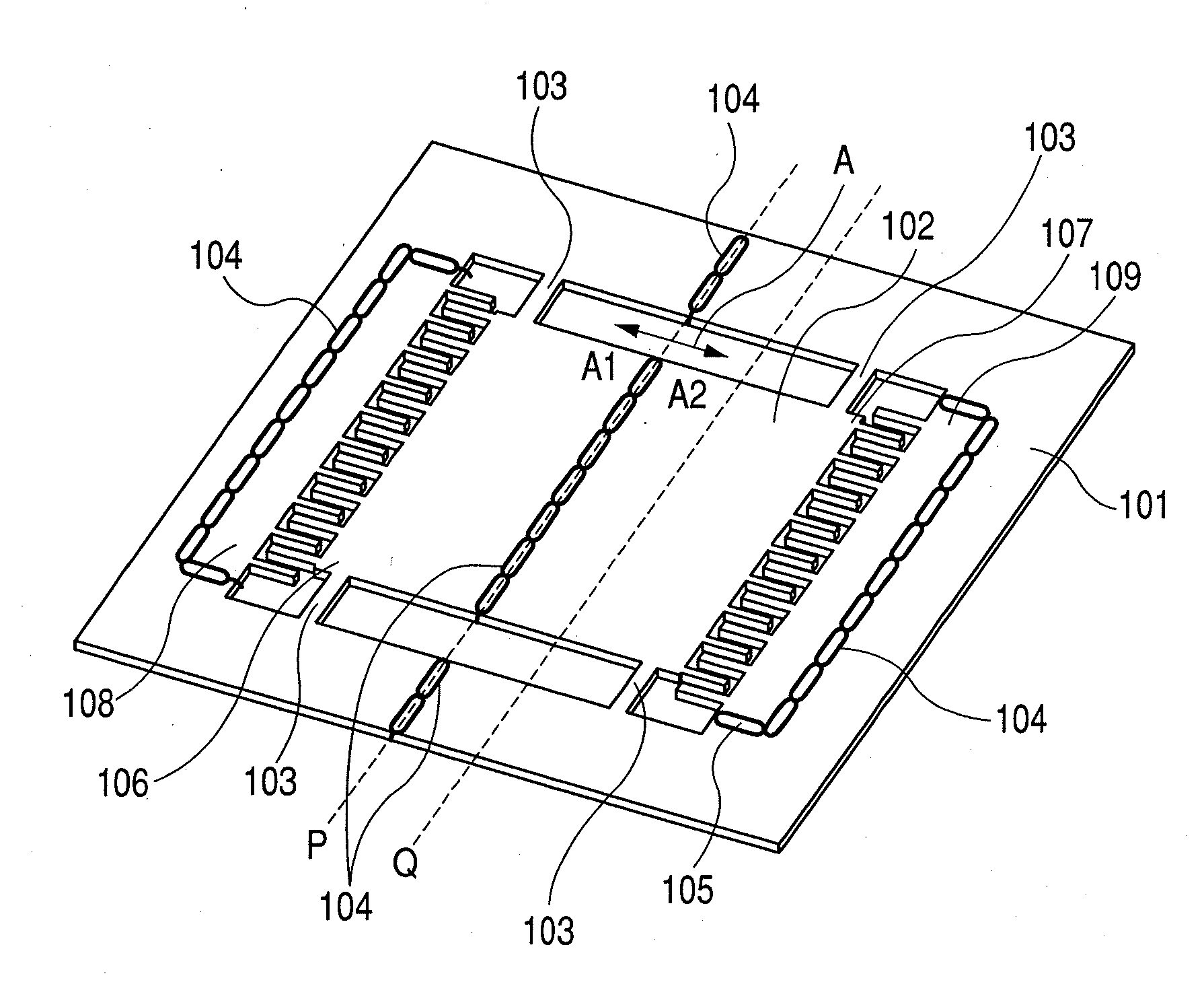
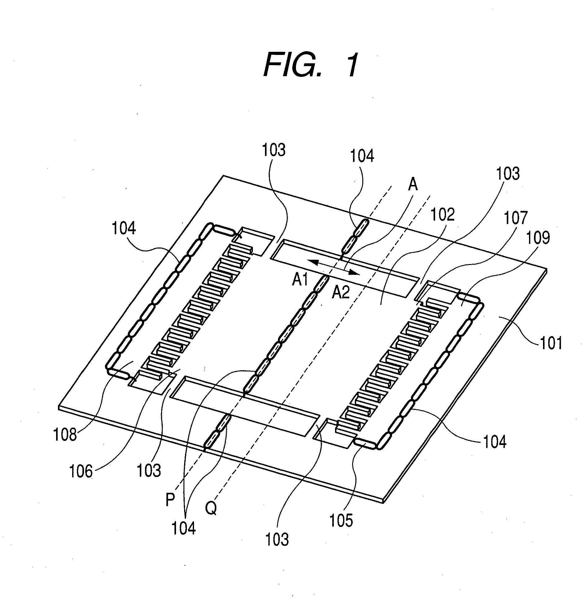
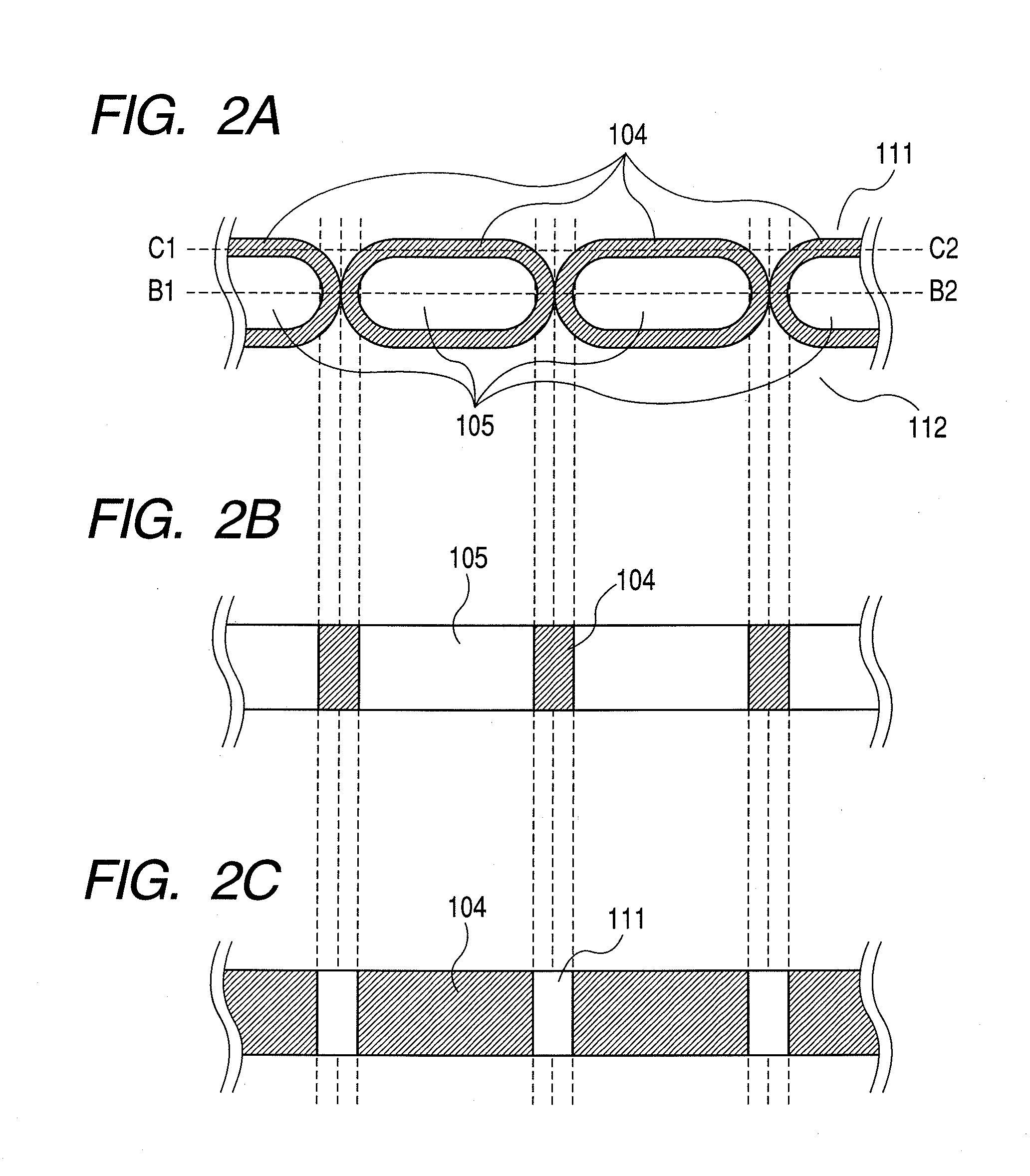
[0046]A first embodiment of the present invention will be described with reference to FIGS. 1, 2A, 2B, 2C, 3-1A to 3-5B, 4A, 4B, and 4C. The first embodiment of the present invention relates to an actuator (mechanism for converting a force of input electric energy into physical motion) including a structural member having a plurality of conductive regions electrically insulated from each other, and to a method of producing the actuator. FIG. 1 is a perspective view of the actuator according to the first embodiment of the present invention. As illustrated in FIG. 1, the actuator includes a substrate 101 of conductive silicon or the like, a movable member 102, beams 103, thermally oxidized films 104 (oxidized regions), through holes 105, a first movable electrode 106, a second movable electrode 107, a first fixed electrode 108, and a second fixed electrode 109.
[0047]The substrate 101 is a base material on which the movable member 102, the beams 103, the fixed electrodes 108 and 109, a...
second embodiment
[0070]Next, a second embodiment of the present invention will be described with reference to FIGS. 5-1 to 5-5B. The second embodiment is different from the first embodiment in the process of producing the actuator. Other structures thereof are substantially the same as those of the first embodiment.
[0071]FIGS. 5-1 to 5-5B are cross-sectional diagrams for illustrating the process of producing the actuator according to the second embodiment of the present invention. Also in FIGS. 5-1 to 5-5B, numeral 201 denotes the silicon, 202 the resist, 203 the mask material, 204 the thermally oxidized film, and 210 the through hole of the oxidized regions. In FIGS. 5-2A to 5-5B, the same components are defined or omitted in the same manner as in FIGS. 3-1A to 3-5B.
[0072]In the second embodiment of the present invention, as illustrated in FIG. 5-1, there is used a substrate (base material) obtained by forming the mask material 203 on both surfaces of the silicon substrate 201. First, the resist 20...
third embodiment
[0080]Next, a third embodiment of the present invention will be described with reference to FIGS. 6-1 to 6-8B. The third embodiment is different from the first embodiment in the process of producing the actuator. Excepting the process, the third embodiment is substantially the same as the first embodiment.
[0081]FIGS. 6-1 to 6-8B are cross-sectional diagrams for illustrating the process of producing the actuator according to the third embodiment of the present invention. In FIGS. 6-1 to 6-8B, numeral 201 denotes the silicon, 202 the resist, 203 the mask material, 204 the thermally oxidized film, 205 an oxidized film, 206 a second silicon substrate, 207 a protective film material, and 210 the through holes of the oxidized regions. In FIGS. 6-2A to 6-8B, the same components are defined or omitted in the same manner as in FIGS. 3-1A to 3-5B.
[0082]In the third embodiment of the present invention, a silicon-on-insulator (SOI) substrate (base material) is used in which the substrate 201 an...
PUM
 Abstract
Description
Claims
Application Information


