Semiconductor integrated circuit and high frequency module with the same

a technology of integrated circuits and high frequency modules, applied in semiconductor devices, electronic switching, pulse techniques, etc., can solve problems such as abnormal increase in harmonic distortion and tx mode, and achieve the effect of reducing the level of harmonics of rf tx output signals

Active Publication Date: 2010-05-13
RENESAS ELECTRONICS CORP
View PDF3 Cites 44 Cited by
  • Summary
  • Abstract
  • Description
  • Claims
  • Application Information

AI Technical Summary

Benefits of technology

[0015]As described in the patent document 3, by driving the gate of the FET of the Tx switch of the antenna switch ANT-SW by the boost output signal of the DC boost circuit, the on resistance of the FET of the Tx switch which is controlled to be on is reduced and, on the other hand, harmonic distortion of the FET of the RX switch which is controlled to be off can be reduced. Further, as described in the patent document 3, the DC control bias and the RF signal are supplied to the DC boost circuit and a DC output bias larger than the DC control bias can be generated from the DC boost circuit, so that an oscillator included in a negative bias generation circuit or a negative circuit as described in the patent document 1 or 2 can be omitted.
[0029]As a result, the on resistance Ron of the FETs 320A to 320D of the first Tx switch 302 of the antenna switch ANT-SW 300 is sufficiently reduced and, as shown in FIG. 15, the RF Tx output signal Pout to be supplied to the antenna ANT coupled to the common I / O port 301 starts increasing.
[0031]In the case where the DC boost output bias VBS of the first DC boost circuit 330 sufficiently rises after lapse of sufficient time since start of the supply of the first RF Tx signal to the first Tx port 306, the gate to source bias Vgs (Rx) of the FETs 360A to 360D of the first Rx switch 304 becomes a deep reverse bias of about −4.5 volts. Therefore, the capacitance value of the gate to source capacitance Cgs (Rx) of the FETs 360A to 360D of the first Rx switch 304 is a sufficiently small value, and a harmonic distortion of the antenna switch ANT-SW can be reduced.
[0036]An object of the present invention is therefore to reduce increase in the level of a harmonic signal of an RF Tx output signal at the time of supplying the RF Tx signal to a bias generation circuit of an antenna switch ANT-SW.
[0044]That is, at the time of supplying the RF Tx signal to the bias generation circuit of the antenna switch ANT-SW, increase in the level of a harmonic signal of an RF Tx output signal can be reduced.

Problems solved by technology

However, when the inventors of the present invention examined the antenna switch ANT-SW described in the patent document 3 in detail prior to the present invention, they found out a problem such that harmonic distortion increases abnormally immediately after switch to the Tx mode.

Method used


Image

  • Semiconductor integrated circuit and high frequency module with the same
  • Semiconductor integrated circuit and high frequency module with the same
  • Semiconductor integrated circuit and high frequency module with the same

Examples


Embodiment Construction

Representative Embodiments

[0062]First, outline of representative embodiments of the present invention disclosed in the application will be described. Reference numerals of the drawings referred to in parentheses in the description of the outline of the representative embodiments merely illustrate components designated with the reference numerals included in the concept of the components.

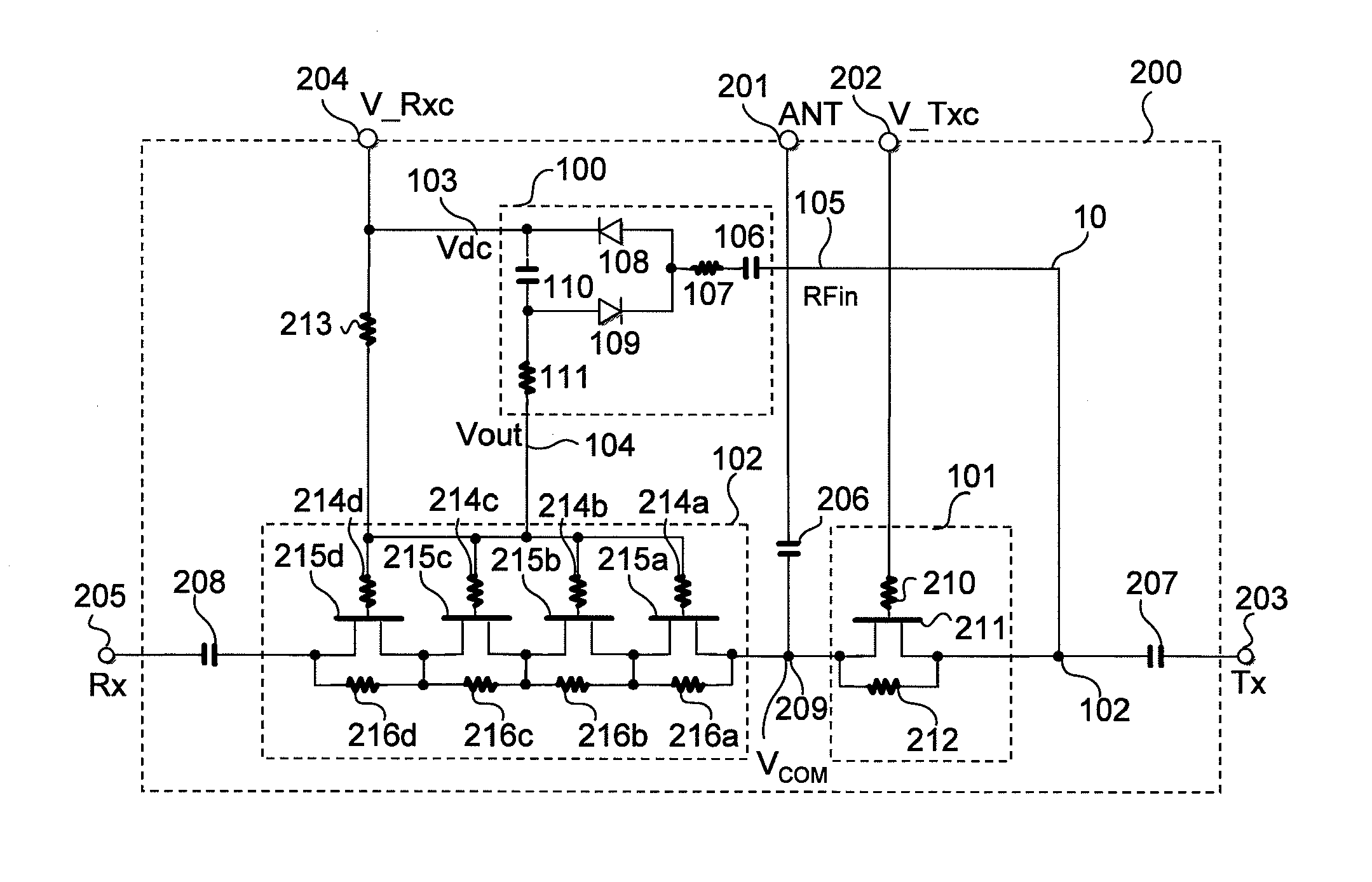
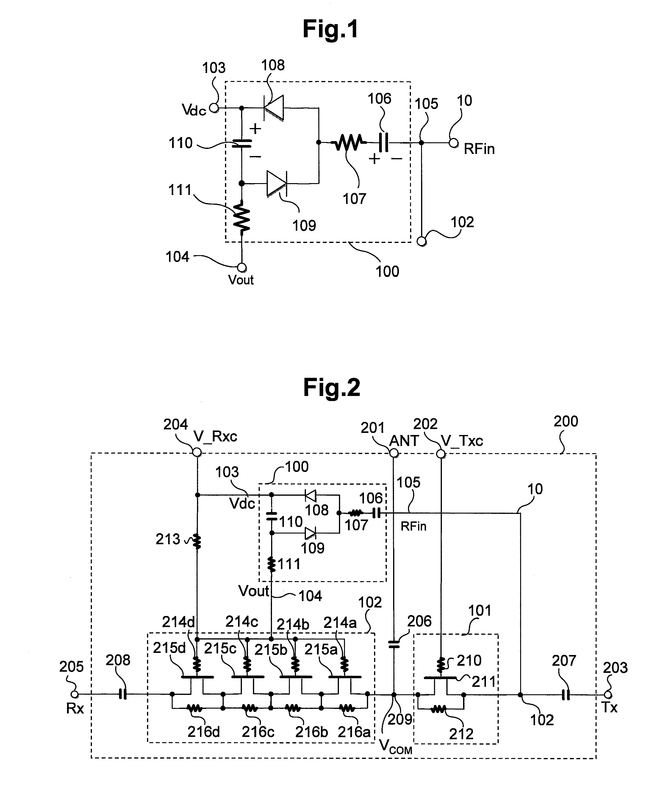
[0063](1) A representative embodiment relates to a semiconductor integrated circuit (200) including at least one antenna switch ANT-SW having a bias generation circuit (100), a transmitter (Tx) switch 101, and a receiver (Rx) switch 102.

[0064]The Tx switch (101) is coupled between a transmitter (Tx) port (203) and an I / O port (201), and an on / off state of a Tx field effect transistor (211) of the Tx switch (101) can be controlled according to level of a Tx control bias (V_Txc) supplied to the Tx control port (202).

[0065]The Rx switch (102) is coupled between the I / O port (201) and a receiver (Rx) por...


PUM


Abstract

The present invention is directed to reduce increase in the level of a harmonic signal of an RF (transmission) Tx output signal at the time of supplying an RF Tx signal to a bias generation circuit of an antenna switch. A semiconductor integrated circuit includes an antenna switch having a bias generation circuit, a Tx switch, and an antenna switch having a bias generation circuit, a transmitter switch, and a receiver (Rx) switch. The on / off state of a transistor of a Tx switch coupled between a Tx port and an I / O port is controlled by a Tx control bias. The on / off state of the transistors of the Rx switch coupled between the I / O port and a receiver (Rx) port is controlled by an RX control bias. A radio frequency (RF) signal input port of the bias generation circuit is coupled to the Tx port, and a negative DC output bias generated from a DC output port can be supplied to a gate control port of transistors of the Rx switch.

Description

CLAIM OF PRIORITY[0001]The present application claims priority from Japanese patent application JP 2008-287921 filed on Nov. 10, 2008, the content of which is hereby incorporated by reference into this application.FIELD OF THE INVENTION[0002]The present invention relates to a semiconductor integrated circuit including an antenna switch ANT-SW and a high frequency module using the same. More particularly, the invention relates to a technique effective to reduce increase in a harmonic signal level of an RF Tx output signal at the time of supplying an RF Tx signal to a bias generation circuit of the antenna switch ANT-SW.BACKGROUND OF THE INVENTION[0003]Hitherto, an antenna switch ANT-SW using a PIN diode is generally used. In recent years, an FET (Field Effect Transistor), particularly, an HEMT (High Electron Mobility Transistor) of a heterojunction structure having low on resistance is used in an antenna switch ANT-SW. By using an FET, an antenna switch ANT-SW can be integrated as a ...

Claims


Application Information

Patent Timeline
Patent Type & Authority Applications(United States)
IPC IPC(8): H03K17/687
CPCH03K17/693H03K17/063
Inventor KATOH, KAORUKOYA, SHIGEKITAKATANI, SHINICHIROSHIGENO, YASUSHINAKAJIMA, AKISHIGEOGAWA, TAKASHI
Owner RENESAS ELECTRONICS CORP
Why Eureka
Try Eureka