Field-effect transistor

a field-effect transistor and transistor technology, applied in the field of field-effect transistors, can solve the problems of reducing on-resistance, limiting the miniaturization techniques of shortening the device gate length, and reducing the threshold voltage, so as to achieve favorable heat dissipation and high heat conductivity

Inactive Publication Date: 2011-06-09
SHARP KK
View PDF15 Cites 36 Cited by
  • Summary
  • Abstract
  • Description
  • Claims
  • Application Information

AI Technical Summary

Benefits of technology

[0016]Accordingly, with the field-effect transistor according to the present invention, because the recessed portion is formed so as to have a snaking shape, the boundary length of the recessed portion (length in the channel widthwise direction) is greater than if the recessed portion were linearly formed in the orthogonal direction. In other words, according to the present invention, increasing the length of the boundary enables the resistance between the source electrode and the drain electrode to be reduced, and enables the current that flows when a constant voltage is applied to the first gate electrode to be increased.
[0032]In this case, heat dissipation is favorable given the high electron saturation velocity, high breakdown voltage and high heat conductivity resulting from employing a nitride compound semiconductor, enabling a field-effect transistor that can operate at high temperature and does not contain harmful substances to be provided.

Problems solved by technology

However, there is a limit to miniaturization techniques for shortening the device gate length due to factors such as the machining accuracy of manufacturing equipment, and the drop in threshold voltage due to short channel effect also becomes problematic as a result of shortening the gate length.
Also, while on-resistance can be reduced as a result of shortening the gate length, as shown in JP 2001-210658A, other problems arise such as the limit to device miniaturization and the drop in threshold voltage due to short channel effect.

Method used


Image

  • Field-effect transistor
  • Field-effect transistor
  • Field-effect transistor

Examples


embodiment 1

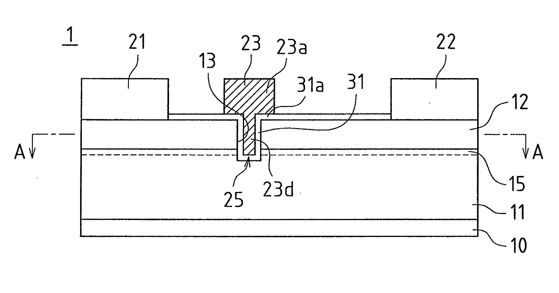
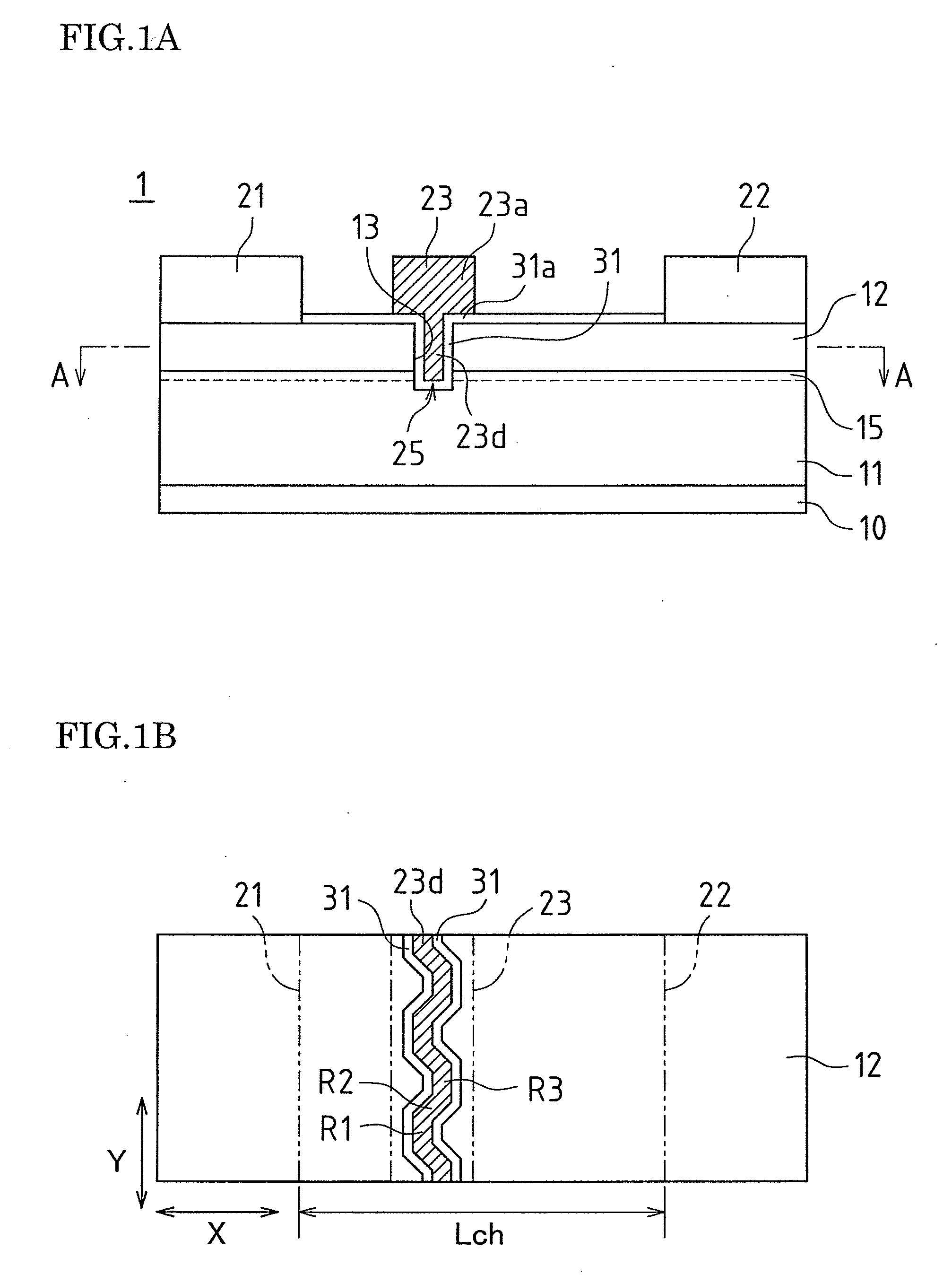
[0067]A field-effect transistor according to Embodiment 1 of the present invention will be described based on FIGS. 1A to 1C.

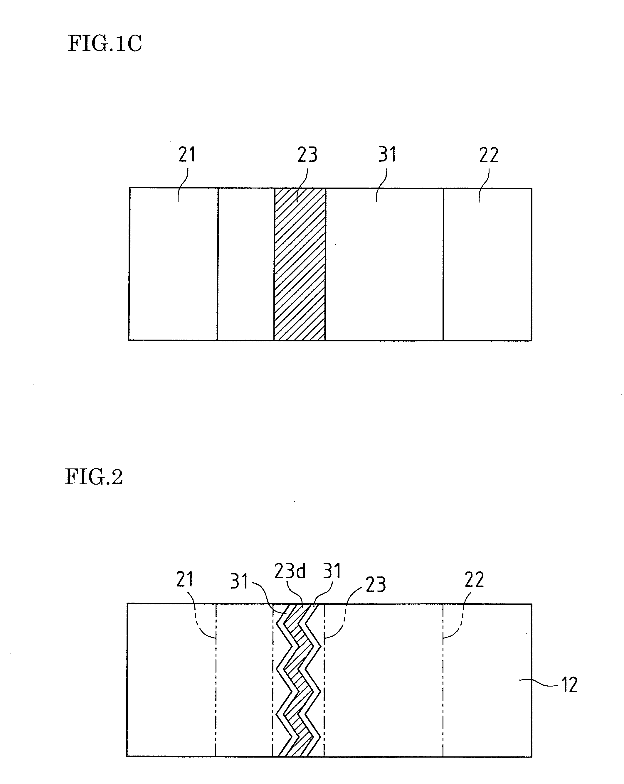
[0068]FIG. 1A is a cross-sectional view of the field-effect transistor according to Embodiment 1 of the present invention. FIG. 1B is a structural plan view showing a cross-section at A-A in FIG. 1A. FIG. 1C is a plan view of the field-effect transistor shown in FIG. 1A. Note that while hatching indicating electrodes has been omitted for ease of viewing, the principal part (first gate electrode 23) has been hatched.

[0069]A field-effect transistor 1 according to the present embodiment is provided with a channel layer 11 formed on a substrate 10, a carrier supply layer 12 formed on the channel layer 11 and forming a heterojunction with the channel layer 11, a recessed portion 13 recessed from a surface of the carrier supply layer 12, a first insulating layer 31 formed along the carrier supply layer 12 and the recessed portion 13 in the range of a channel length ...

embodiment 2

[0119]A field-effect transistor according to Embodiment 2 of the present invention will be described based on FIGS. 9A to 9C. Note that the same reference numerals are given to constituent elements having a similar function to Embodiment 1, and description thereof will be omitted.

[0120]FIG. 9A is a cross-sectional view of a field-effect transistor according to Embodiment 2 of the present invention. FIG. 9B is a structural plan view of the field-effect transistor, showing a cross-section at B-B in FIG. 9A. FIG. 9C is a plan view of the field-effect transistor shown in FIG. 9A. Note that that while hatching has been omitted for ease of viewing, the principal parts (first gate electrode 23, second gate electrode 24) have been hatched.

[0121]A field-effect transistor 2 according to present embodiment is provided with a channel layer 11 formed on a substrate 10, a carrier supply layer 12 formed on the channel layer 11 and forming a heterojunction with the channel layer 11, a recessed port...


PUM


Abstract

A field-effect transistor provided with a channel layer, a carrier supply layer forming a heterojunction with the channel layer, a recessed portion recessed from a surface of the carrier supply layer, a first insulating layer formed at least along the recessed portion, a first gate electrode formed on the first insulating layer, a source electrode formed on one side of the recessed portion in a channel lengthwise direction, and a drain electrode formed on an opposite side of the recessed portion in the channel lengthwise direction. The recessed portion snakes in a direction intersecting the channel lengthwise direction, in the range of a channel length between the source electrode and the drain electrode.

Description

BACKGROUND OF THE INVENTION[0001]This application claims priority under 35 U.S.C. §119(a) on Patent Application No. 2009-278727 filed in Japan on Dec. 8, 2009, the entire contents of which are herein incorporated by reference.[0002]The present invention relates to a field-effect transistor, and more particularly to a field-effect transistor with a heterostructure.[0003]Heterostructure field-effect transistors have attracted attention as key devices for next-generation power electronics. Demand for field-effect transistors with increased breakdown voltage and increased current capability has further grown.[0004]FIG. 10 is a structural view of an example of a conventional HFET (Heterostructure Field-Effect Transistor) employing a heterojunction. The conventional HFET has a channel layer 111 and a carrier supply layer 112 sequentially formed on a substrate 110. A source electrode 121 and a drain electrode 122 are formed as electrodes on the carrier supply layer 112, and an insulating l...

Claims


Application Information

Patent Timeline
Patent Type & Authority Applications(United States)
IPC IPC(8): H01L29/78H01L29/205
CPCH01L29/2003H01L29/7787H01L29/4236H01L29/402
Inventor NAGAHISA, TETSUZOTWYNAM, JOHN KEVIN
Owner SHARP KK
Why Eureka
Try Eureka