

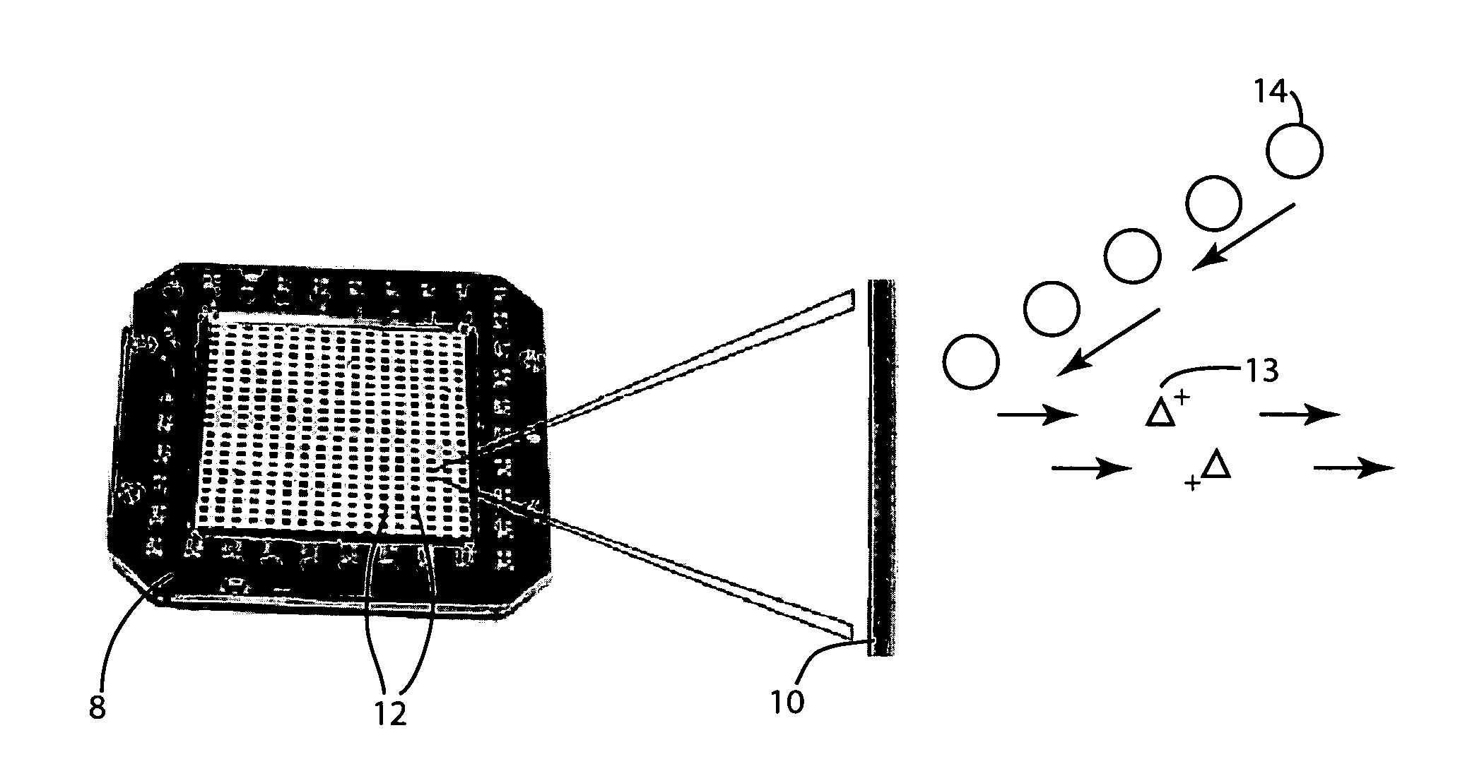
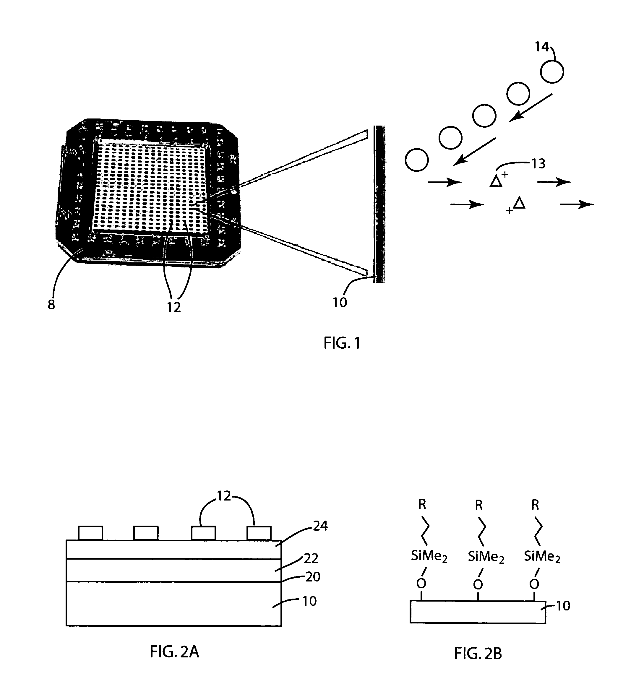
Nanostructured thin films and their uses
a thin film, nanotechnology, applied in the field of nanotechnology, can solve the problems of difficult analysis of samples with low molecular weights with maidi, large degree of chemical noise to be observed at m/z ratio, and the use of silicon nanowires as substrate surfaces may pose some challenges in reproducible manufacturing of such surfaces, etc., to achieve simple and inexpensive manufacturing processes, improve the effect of surface area and high uniformity
- Summary
- Abstract
- Description
- Claims
- Application Information
AI Technical Summary
Benefits of technology
Problems solved by technology
Method used
Image

Examples
example 1
[0068]The following non-limiting example demonstrates the feasibility of using an alumina nanostructured underlying thin film coated with an active silicon layer to perform mass spectrometry analysis. The nanostructured surface used in these experiments is based on alumina. 50 nm of alumina was sputtered onto a 40 nm square polished stainless steel plate. The plate was exposed to boiling water for three minutes which converts the alumina into a highly structured surface.
[0069]The plate was then oxygen plasma cleaned for 10 minutes before placing it into a CVD furnace where silicon was deposited on it for 70 minutes. Two steel plates without the nanostructured alumina were also placed into the furnace as controls, one with no coating (FIG. 5A) and the other with a silicon film layer deposited thereon but no underlying alumina nanostructured surface (FIG. 5B). When the plates were removed from the furnace they were exposed to trichloro-perfluoro octyl silane (Gelest, Morrissville, Pa....
example 2
[0072]The following non-limiting example demonstrates the feasibility of using an aluminum nanostructured underlying thin film coated with an active tungsten layer to perform mass spectrometry analysis. The nanostructured surface used in these experiments is based on aluminum. 100 nm of aluminum was sputtered onto a 40 mm square polished stainless steel plate. The plate was exposed to boiling water for five minutes which converts the aluminum into a highly structured surface.
[0073]The plate was then oxygen plasma cleaned for 10 minutes before placing it into a high vacuum sputtering system (UHV Sputtering Inc., San Jose, Calif.) where tungsten was deposited on it to a depth of 50 nm. The plate was then plasma cleaned again and was exposed to trichloro-perfluoro octyl silane (Gelest, Morrisville, Pa.) vapor for three hours to render it hydrophobic. The plate was then washed thoroughly in methanol and baked for 20 minutes at 100 degrees Celsius. The plate was spotted with 25 pg of pra...
PUM
| Property | Measurement | Unit |
|---|---|---|
| thickness | aaaaa | aaaaa |
| thickness | aaaaa | aaaaa |
| thickness | aaaaa | aaaaa |
Abstract
Description
Claims
Application Information