Production method of liquid crystal display device and liquid crystal display device
a production method and liquid crystal display technology, applied in the field production methods of liquid crystal display devices, can solve the problems of affecting the image display in the display region, deterioration, and change in characteristics of switching elements, and achieve the effect of suppressing light leakage from the frame region
- Summary
- Abstract
- Description
- Claims
- Application Information
AI Technical Summary
Benefits of technology
Problems solved by technology
Method used
Image

Examples
embodiment 1
[0193]FIG. 1 is a plan view schematically showing a liquid crystal display panel in accordance with Embodiment 1.
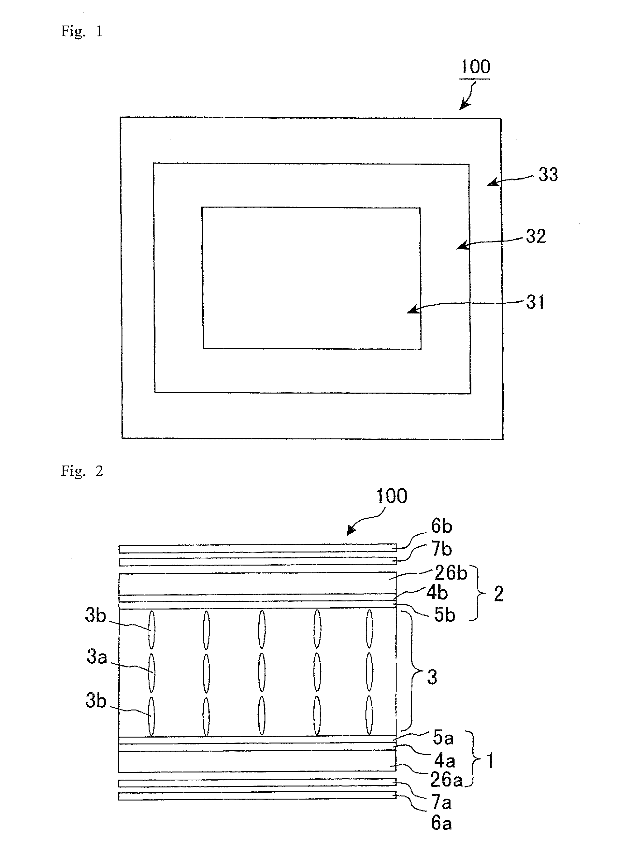
[0194]A liquid crystal display panel 100 in the present Embodiment has a display region (effective display area) 31 and a frame region 32 surrounding the display region 31 (non-display region, non-effective display area) in a substrate plane, as shown in FIG. 1. The display region 31 has a square shape and the frame region 32 has a band-shape, as viewed in plane. The display region 31 is a region where images are displayed and it is constituted by a plurality of pixels arrayed in a matrix pattern. The frame region 32 is a region which has no contribution to display and it is arranged around the display region. The display region 31 includes a light-shielding region that is arranged around and / or inside each pixel. The liquid crystal display panel 100 has, around the frame region 32, a terminal region (substrate extending part) 33 where a plurality of terminals through whi...
embodiment 2
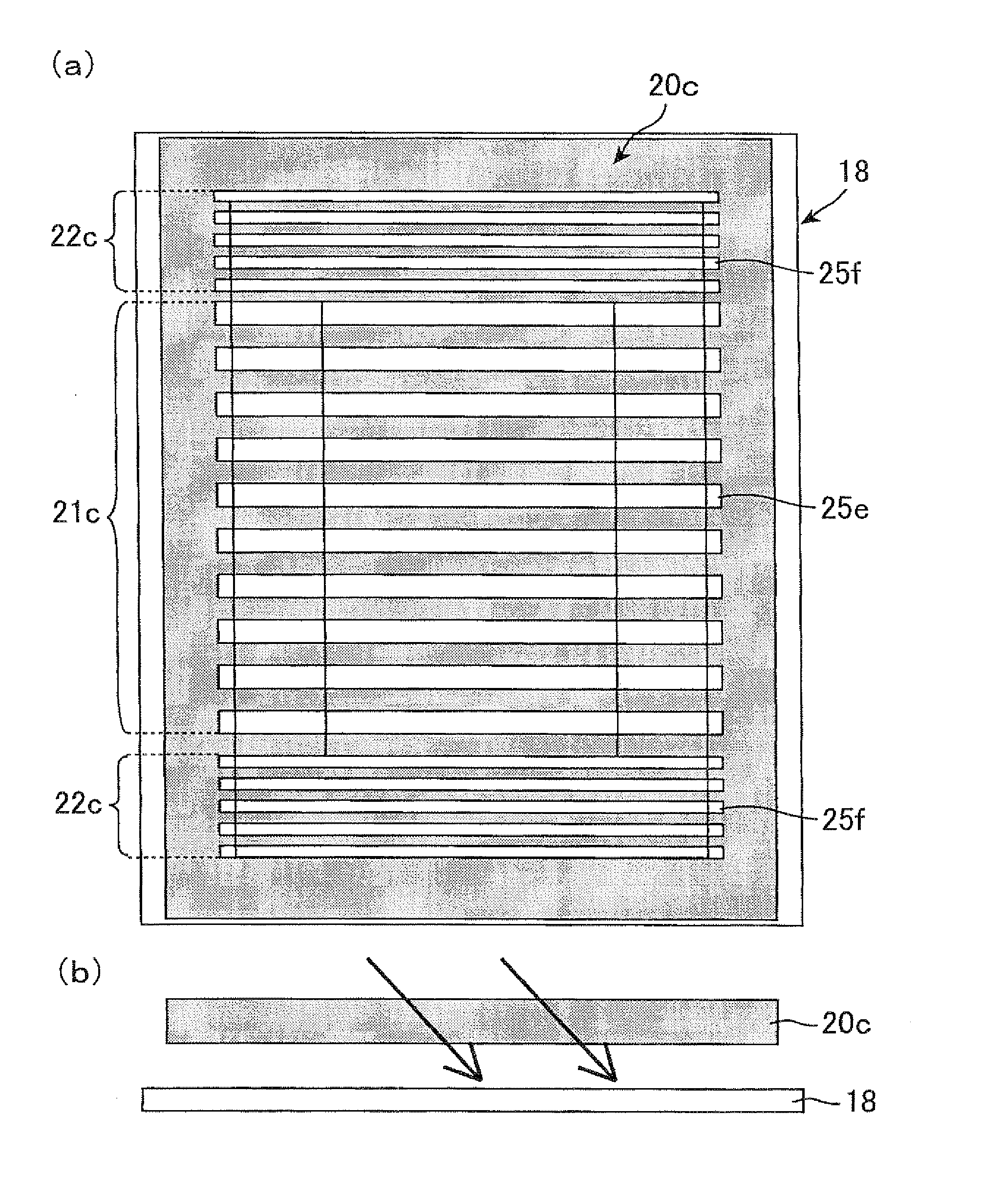
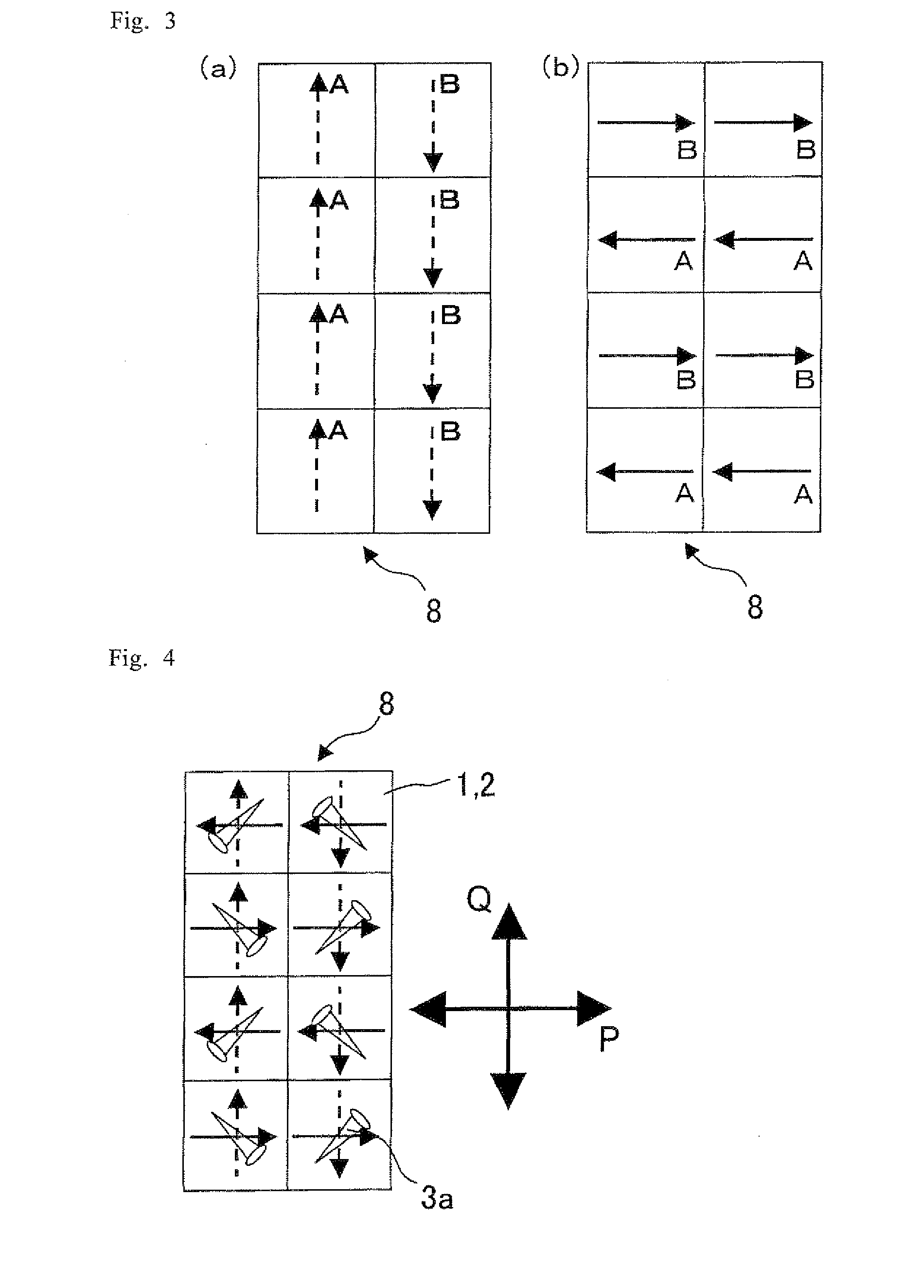
[0234]Embodiment 2 is mentioned below. The overlapping contents between the present Embodiment and Embodiment 1 are omitted and not shown in drawings because a difference between the two is just an embodiment of the slits through which the frame region is exposed of the photomask. FIG. 15 is a schematic view showing an embodiment of exposure for an alignment film (a second substrate) in the exposure step (the 1st scan) in accordance with Embodiment 2. FIG. 15(a) is a plan view of a photomask. FIG. 15(b) is a plan view of the second substrate. FIG. 16 is a schematic view showing an embodiment of exposure for the alignment film (the second substrate) in the exposure step (the 2nd scan) in accordance with Embodiment 2. FIG. 16(a) is a plan view of the photomask. FIG. 16(b) is a plan view of the second substrate. FIG. 17 is a plan view schematically showing one picture element in a display region of a liquid crystal display panel in accordance with Embodiment 2. FIG. 17(a) shows a direc...
embodiment 3
[0244]Embodiment 3 is mentioned below. The overlapping contents between the present Embodiment and Embodiments 1 and 2 are omitted and are not shown in drawings because a difference between the two is just an embodiment of the transmissive parts through which the frame region is exposed of the photomask. FIG. 19 is a schematic view showing an embodiment of exposure for an alignment film (a second substrate) in the exposure step (the 1st shot) in accordance with Embodiment 3. FIG. 19(a) is a plan view of a photomask. FIG. 19(b) is a plan view of the second substrate. FIG. 20 is a schematic view showing an embodiment of exposure for the alignment film (the second substrate) in the exposure step (the 2nd shot) in accordance with Embodiment 3. FIG. 20(a) is a plan view of the photomask. FIG. 20(b) is a plan view of the second substrate. FIG. 21 is a plan view schematically showing one picture element in a display region of a liquid crystal display panel in accordance with Embodiment 3. ...
PUM
| Property | Measurement | Unit |
|---|---|---|
| angle | aaaaa | aaaaa |
| angle | aaaaa | aaaaa |
| pretilt angle | aaaaa | aaaaa |
Abstract
Description
Claims
Application Information