Method of manufacturing semiconductor devices

a manufacturing method and technology of semiconductor devices, applied in the direction of semiconductor devices, basic electric elements, electrical appliances, etc., can solve the problems of reducing the reliability of optical semiconductor devices, affecting the operation of semiconductor devices, and affecting the quality of semiconductor films, so as to reduce the process time

Inactive Publication Date: 2010-05-13
STANLEY ELECTRIC CO LTD
View PDF3 Cites 20 Cited by
  • Summary
  • Abstract
  • Description
  • Claims
  • Application Information

AI Technical Summary

Benefits of technology

[0011]According to the method of manufacturing semiconductor devices of the present invention, in order to form the streets along device division lines in the semiconductor film laid over the metal support, the dry etching and the wet etching are used in combination. At the stage of etching the semiconductor film until the metal support is exposed, the wet etching is used, and hence the problem can be avoided that the metal support is exposed to plasma and that thus metal particles sputtered from the constituting the metal support scatter to stick to the semiconductor film, resulting in a leak current or a short. Further, because the flattening process is performed on the semiconductor film prior to each of the etchings, so that the surface state of the semiconductor film becomes uniform, the occurrence of etching residue on the streets after the wet etching can be prevented. Yet further, by using the dry etching (RIE: Reactive ion etching) in the first half of the street forming process, the process time can be reduced.

Problems solved by technology

A decrease in the reliability of the optical semiconductor device due to, for example, a decrease in efficiency and degradation of the semiconductor film is posing a problem.
Metal particles sticking to the side of the semiconductor film, especially at or near the active layer may cause a current at operation to flow through the sticking metal particles, resulting in a leak current or a short.
This sticking metal is difficult to remove even by acid treatment or the like, and cannot be removed unless part of the semiconductor film is scraped off.
It is practically impossible to control to finish dry etching just when the metal support is exposed so as to prevent the scattering of metal particles because of the flatness of the metal support.
However, according to a study by the inventors of the present invention, it is made clear that performing wet etching on the semiconductor layer (n-type semiconductor layer) exposed by removing the growth substrate cannot completely remove the intended part of the semiconductor film, and that thus etching residue occurs.
Further, after the growth substrate is removed by LLO (laser lift-off) and so on, the surface of the semiconductor has laser traces and dislocations produced at crystal growth with various crystal planes or faces being exposed and non-uniformly distributed.
This is thought to be because the semiconductor film has partially deteriorated due to the laser irradiation in the LLO process, so that the etching rate of the deteriorated portions of the semiconductor film has decreased.
When laser scribing is performed to divide the metal support with etching residues occurring on a street, laser beam will be scattered by the residues of the semiconductor film on the street, and therefore the metal support cannot be cut.
Although it is thought to be able to address the problem of etching residue by raising the temperature of the etchant or lengthening the process time in this method, the semiconductor film will be damaged and in addition the process time will become longer, which are not preferable.
However, the resist will be degraded, and in addition side etching under the resist may occur when wet etching is performed under conditions of relatively high reactivity as mentioned above.

Method used


Image

  • Method of manufacturing semiconductor devices
  • Method of manufacturing semiconductor devices
  • Method of manufacturing semiconductor devices

Examples


Embodiment Construction

[0017]An embodiment of the present invention will be described below with reference to the drawings. The same reference numerals are used to denote substantially the same or equivalent constituents or parts throughout the figures cited below.

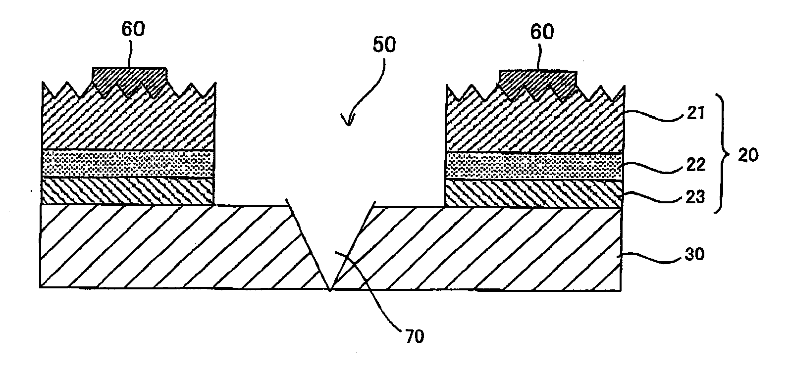
[0018]FIGS. 3A to 3I are cross-sectional views of optical semiconductor devices in process steps respectively of the manufacturing process according to the embodiment of the present invention. FIG. 4 is a process flow diagram showing a method of manufacturing an optical semiconductor device that is the embodiment of the present invention.

(Semiconductor Layer Growing Process, Step S10)

[0019]A substrate used for crystal growth (hereinafter, referred to as growth substrate) is prepared. In the present embodiment, a C-plane sapphire substrate 10 is used on which a semiconductor film made of AlxInyGazN (0≦x≦1, 0≦y≦1, 0≦z≦1, x+y+z=1) can be formed by an MOCVD method (metal organic chemical vapor deposition method). The layers constituting a semiconduc...


PUM


Abstract

A growth substrate is removed from a semiconductor film, and a surface of the semiconductor film exposed by removing the growth substrate is flattened. The semiconductor film along device division lines are partially etched by dry etching to form grooves in a lattice that form streets, not reaching the metal support in the semiconductor film. The surface of the semiconductor film at the bottom of the grooves is flattened. The semiconductor film along the device division lines at the bottom of the grooves are further etched by wet etching to expose the metal support at the bottom of the grooves to finish the streets.

Description

BACKGROUND OF THE INVENTION[0001]1. Field of the Invention[0002]The present invention relates to a method of manufacturing semiconductor devices and particularly to a technique of forming grooves (streets) separating individual semiconductor devices in a semiconductor film formed over a metal support.[0003]2. Description of the Related Art[0004]Optical semiconductor devices such as light emitting diodes have advanced to be of high efficiency and high output power due to the recent years' progress in technology. However, with the output power having become higher, the amount of heat produced in the optical semiconductor device has increased. A decrease in the reliability of the optical semiconductor device due to, for example, a decrease in efficiency and degradation of the semiconductor film is posing a problem. In order to solve the problem, the semiconductor device is configured such that a growth substrate (i.e., a substrate used for crystal growth) which is relatively low in hea...

Claims


Application Information

Patent Timeline
Patent Type & Authority Applications(United States)
IPC IPC(8): H01L21/20
CPCH01L21/0242H01L21/0254H01L33/0095H01L33/0079H01L21/0262H01L33/0093
Inventor TANAKA, SHINICHISAITO, TATSUYAYOKOBAYASHI, YUSUKE
Owner STANLEY ELECTRIC CO LTD
Why Eureka
Try Eureka