Power semiconductor module

a technology of semiconductor modules and semiconductor chips, applied in semiconductor devices, semiconductor/solid-state device details, electrical devices, etc., can solve the problems of reducing radiation efficiency, adversely affecting chip parts, and peeling off of semiconductor chips, so as to reduce radiation efficiency and suppress warpage of ceramic substrates.

Active Publication Date: 2010-05-27
SANSHA ELECTRIC MFG
View PDF4 Cites 9 Cited by
  • Summary
  • Abstract
  • Description
  • Claims
  • Application Information

AI Technical Summary

Benefits of technology

[0015]According to the present invention, thermal expansion characteristics of both surfaces of a ceramic substrate can be made uniform to suppress warpage of the ceramic substrate. Also, resin intruding onto a metal layer can be accommodated in a groove part, and therefore a reduction in radiation efficiency due to attachment of the resin onto a surface of an inner pattern can be prevented.

Problems solved by technology

For this reason, if, due to a difference in a thermal expansion coefficient between the ceramic substrate and the resin, mold shrinkage of the resin, or warpage of the substrate caused by a heat cycle during operation occurs, the occurrence causes a reduction in radiation efficiency, or peeling-off of a semiconductor chip.
However, in the case where the silicone gel is used to protect the chip parts, moisture intruding from a gap of the case may adversely influence the chip parts.
Also, electrical connections among the chip parts are made with wire bonding, soldering of a lead frame, or ultrasonic bonding; however, if a part of the bonding is deteriorated by heat or the like, the use of the silicone gel as a protecting material makes it difficult to stably fix the wire or lead frame.

Method used


Image

  • Power semiconductor module
  • Power semiconductor module
  • Power semiconductor module

Examples


Embodiment Construction

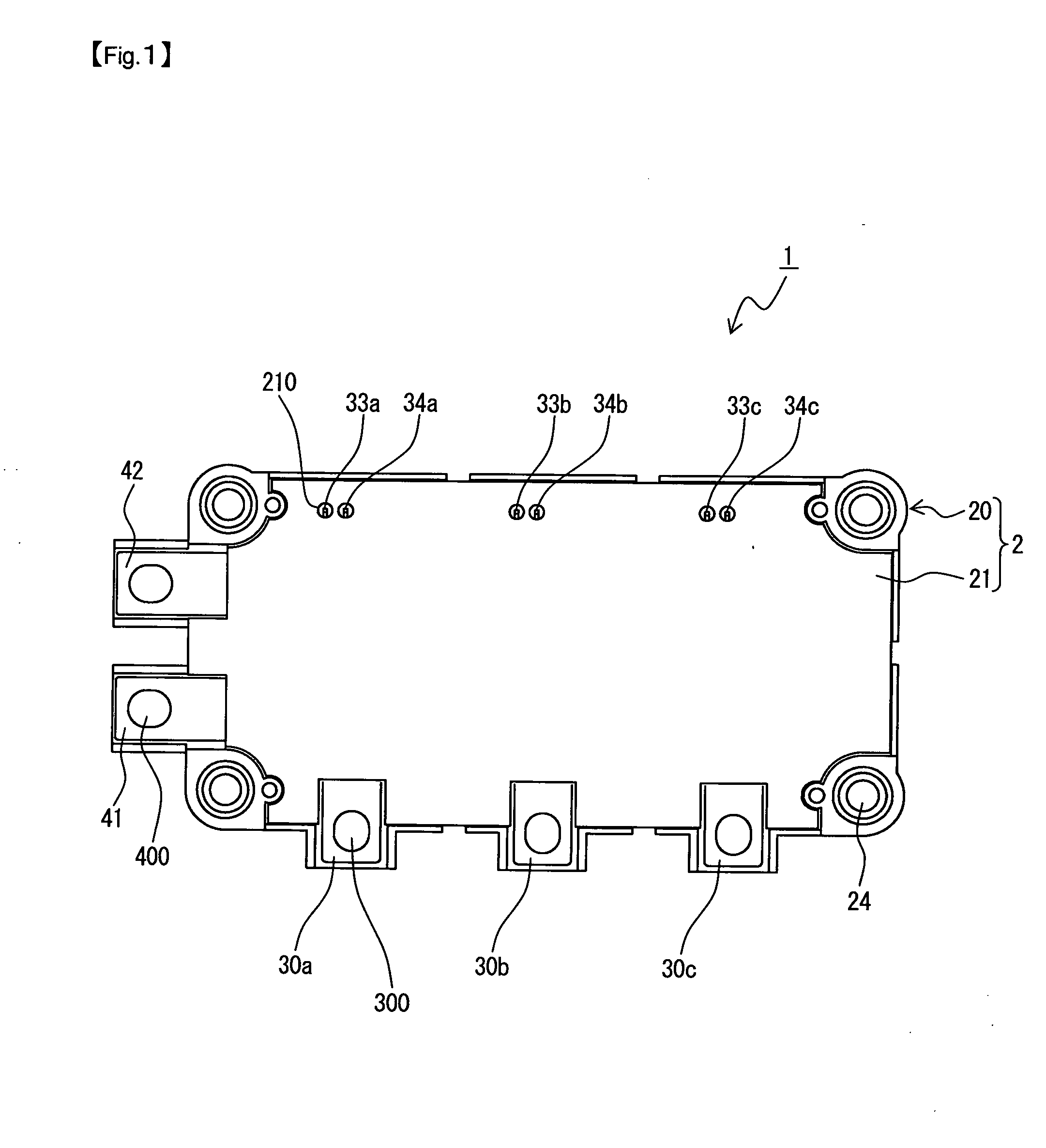
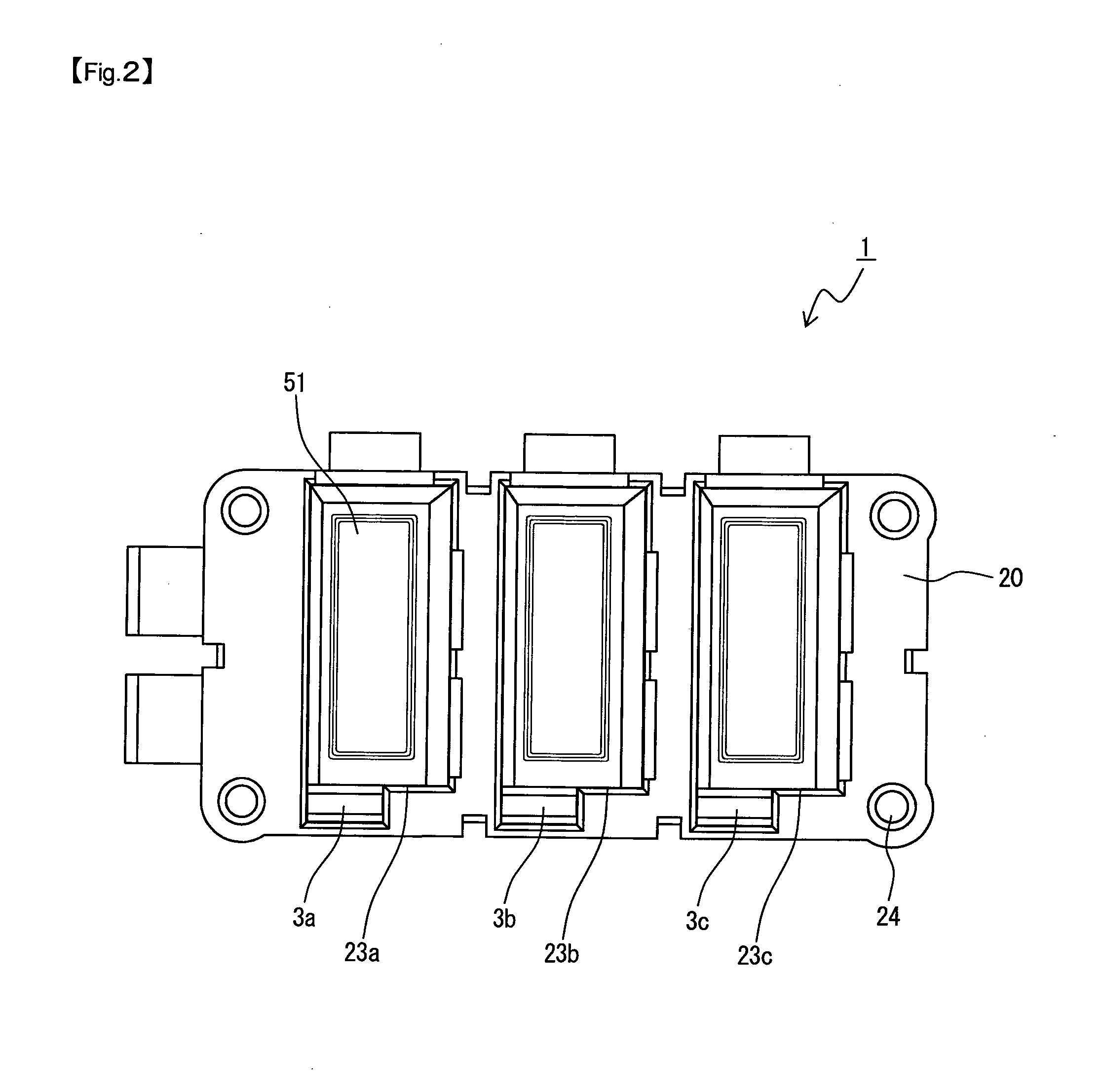
[0016]FIGS. 1 and 2 are appearance diagrams illustrating one configuration example of a semiconductor module 1 according to an embodiment of the present invention, in which FIG. 1 illustrates a top surface, and FIG. 2 a bottom surface. FIG. 3 is a development perspective view illustrating an appearance upon assembly of the semiconductor module 1.

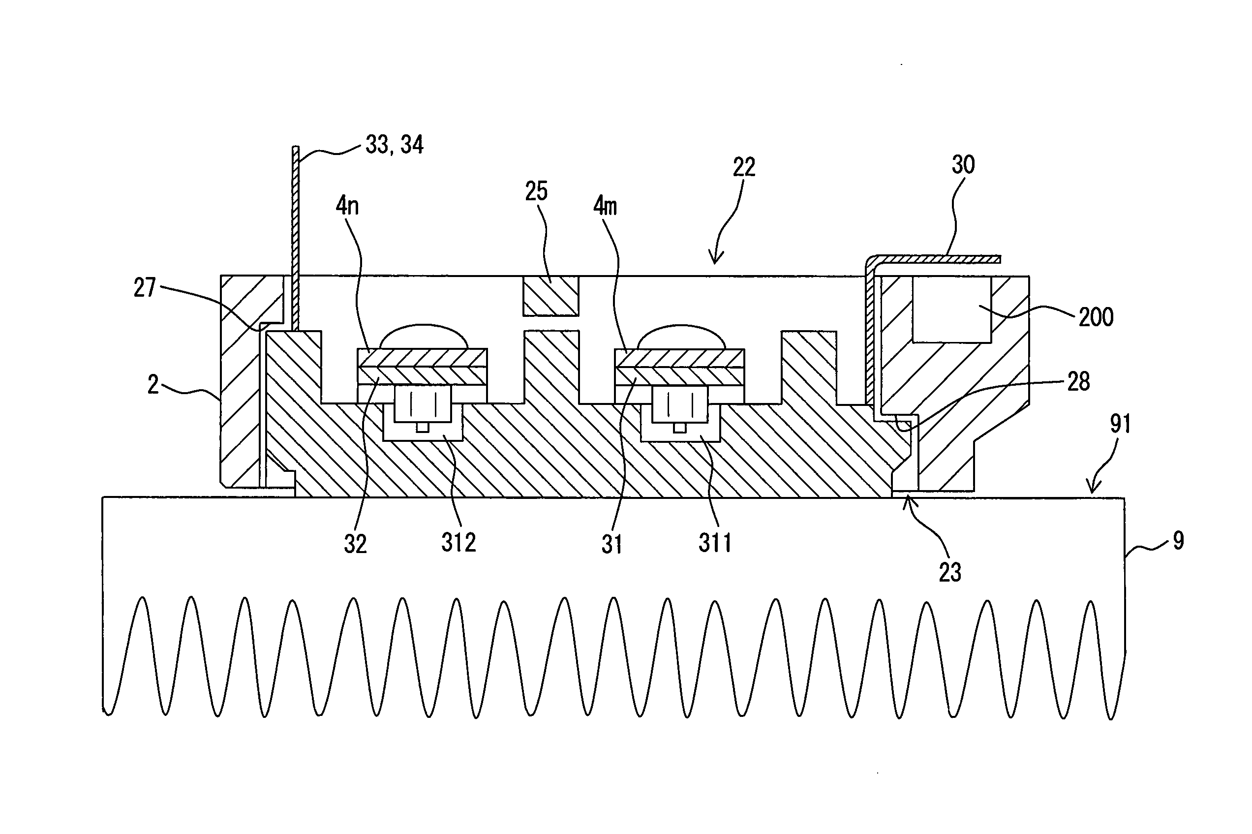
[0017]The semiconductor module 1 is a power semiconductor module intended to convert AC power and DC power with use of semiconductor elements such as a thyristor, diode, and bipolar transistor. In the present embodiment, as an example of such a power semiconductor module, there is described a module for achieving a bridge circuit with use of three thyristors and three diodes. Such a bridge circuit is widely used for a three-phase AC converter that full-wave rectifies a three-phase AC power supply to convert it into a DC power supply.

[0018]The semiconductor module 1 is configured to contain three common units 3 (3a to 3c) and two metal plates...


PUM


Abstract

[Summary]
[Object] To suppress warpage of a ceramic substrate, and to prevent a reduction in radiation efficiency.
[Means for Settlement] A power semiconductor module includes a module casing fitted with a radiator, and a common unit retained by the module casing. The common unit has: a ceramic substrate having a circuit surface disposed with a semiconductor element, and a radiation surface brought into abutting contact with the radiator; and a package formed by exposing the radiation surface and sealing the circuit surface with heat resistant resin. The circuit surface and the radiation surface are respectively formed of metal layers 51 formed on the ceramic substrate, and the metal layer 51 forming the radiation surface has: by forming a buffer pattern 512 including a groove part extending along a circumferential part thereof, a radiation pattern 510 formed on an inner side of the buffer pattern 512; and an outer peripheral pattern 511 formed on an outer side of the buffer pattern 512. Such a configuration enables warpage of the ceramic substrate to be suppressed, and a reduction in radiation efficiency to be prevented.

Description

TECHNICAL FIELD[0001]The present invention relates to a power semiconductor module, and more particularly, to a power semiconductor module used for an electrical power converter such as a converter or inverter.BACKGROUND ART[0002]As a semiconductor module, there is known a device in which a semiconductor element used for an electrical power converter is sealed with resin and modularized. In this sort of semiconductor module, a chip arrangement surface of a ceramic substrate is sealed with resin, and heat is radiated from a back surface of the ceramic substrate. For this reason, if, due to a difference in a thermal expansion coefficient between the ceramic substrate and the resin, mold shrinkage of the resin, or warpage of the substrate caused by a heat cycle during operation occurs, the occurrence causes a reduction in radiation efficiency, or peeling-off of a semiconductor chip.[0003]Because of this, in a typical semiconductor module, a ceramic substrate on which chip parts includi...

Claims


Application Information

Patent Timeline
Patent Type & Authority Applications(United States)
IPC IPC(8): H01L23/34
CPCH01L23/3735H01L25/072H01L2924/3511H01L2924/0002H01L2924/00H01L23/36
Inventor SODA, OSAMUOHNISHI, YUKIINAMI, KAZUNORIUCHIDA, TOSHIO
Owner SANSHA ELECTRIC MFG
Why Eureka
Try Eureka