Organic electroluminescent display device and method and apparatus of manufacturing the same

a technology of electroluminescent display and organic electroluminescent, which is applied in the manufacture of electrode systems, electric discharge tubes/lamps, discharge tubes luminescent screens, etc., can solve the problems of short response time, high brightness, and wide viewing angle of oeld devices, and achieve the effect of improving display quality and production efficiency

Active Publication Date: 2010-05-27
LG DISPLAY CO LTD
View PDF22 Cites 23 Cited by
  • Summary
  • Abstract
  • Description
  • Claims
  • Application Information

AI Technical Summary

Benefits of technology

[0029]An advantage of the present invention is to provide an organic electroluminescent display device and a method and an apparatus of manufacturing the same that can improve display quality and production efficiency.
[0030]Additional features and advantages of the present invention will be set forth in the description which follows, and in part will be apparent from the description, or may be learned by practice of the invention. These and other advantages of the invention will be realized and attained by the structure particularly pointed out in the written description and claims hereof as well as the appended drawings.
[0031]To achieve these and other advantages and in accordance with the purpose of the present invention, as embodied and broadly described herein, an organic electroluminescent display device includes an array substrate including a driving thin film transistor in a pixel region on a first substrate; an opposing substrate including an organic electroluminescent diode in the pixel region on a second substrate; an adhesive layer filling a space between the array substrate and the opposing substrate; and a connection spacer to electrically connect the organic electroluminescent diode with the driving thin film transistor.
[0032]In another aspect, an apparatus of manufacturing an organic electrolu

Problems solved by technology

Further, the OELD devices have fast response time, high brightness, and wide viewing angles.
However, the OELD device having the empty space is weak to exterior impact or pressure, and contact defects between the organic electroluminescent diode E and the driving thin film transistor Td are thus frequently caused.
Accordingly, it is difficult for the OELD device 1 to obtain long lifetime.
Accordingly, the moisture permeates into the not-covered portion of the organic electroluminescent diode E, and defects thus occur.
Further, in the process of forming the passivation layer or the metal layer, impurities of several micrometers are frequ

Method used


Image

  • Organic electroluminescent display device and method and apparatus of manufacturing the same
  • Organic electroluminescent display device and method and apparatus of manufacturing the same
  • Organic electroluminescent display device and method and apparatus of manufacturing the same

Examples


first embodiment

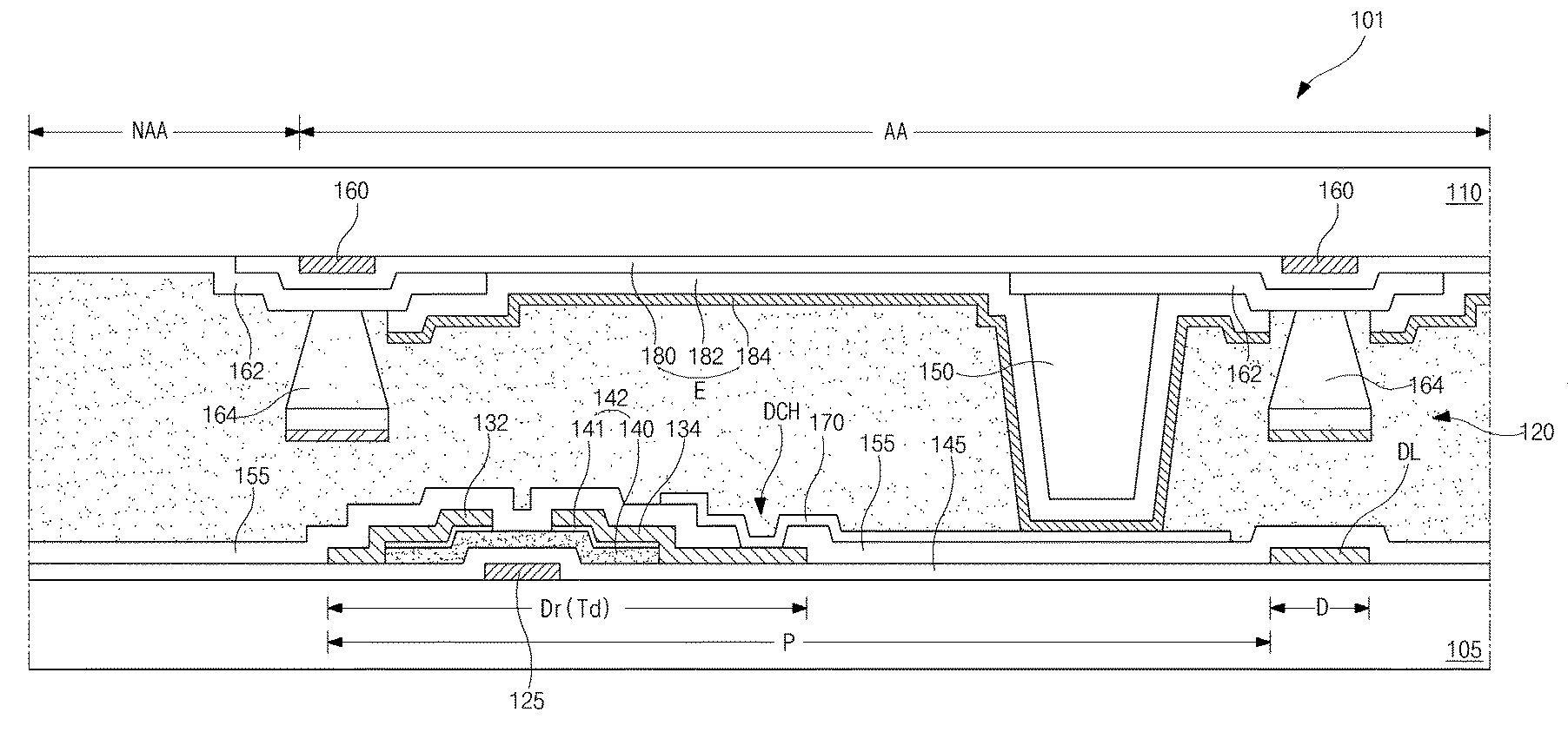
[0052]FIG. 3 is a cross-sectional view illustrating a dual plate type OELD device according to the present invention.

[0053]Referring to FIG. 3, the OELD device 101 includes an array substrate and an opposing substrate. The OELD device 101 includes a display region AA to display images and a non-display region NAA. The non-display region NAA is a peripheral region of the OELD device 101. The non-display region NAA may surround the display region AA. The display region AA may include a plurality of pixel regions P in a matrix form.

[0054]The array substrate includes a gate line (not shown) and a data line DL on a first substrate 105 to cross each other to define the pixel region P. The data line DL is formed in a data region D. In the pixel region P, a switching thin film transistor (not shown) and a driving thin film transistor Td are formed. The switching thin film transistor is connected to the corresponding gate line and data line DL. The driving thin film transistor Td is formed i...

second embodiment

[0098]FIG. 7A is a schematic plan view illustrating an OELD device according to the present invention, and FIGS. 7B and 7C are pictures, of first to fourth regions of the OELD device of FIG. 7A, taken in reliability tests on the OELD device.

[0099]Referring to FIG. 7A, the OELD device includes an array substrate and an opposing substrate with an adhesive layer therebetween. The OELD device includes a display region AA and a non-display region surrounding the display region NAA. A seal pattern 290 is at the non-display region NAA.

[0100]FIG. 7B shows lighting statuses of first to fourth regions (1) to (4) of the OELD device at a first elapsed time after the OELD device is transferred into a chamber under conditions that a temperature is about 80° C. and a humidity is about 95%, and FIG. 7C shows lighting status of first to fourth regions (1) to (4) of the OELD device at a second elapsed time after the OELD device is transferred into a chamber under conditions that a temperature is abou...

third embodiment

[0107]FIGS. 9A and 9B are pictures, of two corner regions of each of OELD devices according to the present invention, taken in reliability tests on the OELD devices.

[0108]The test of FIG. 9A is made on an OELD device which has three shield patterns 386 having a width of about 60 μm, and the two corners (1) and (2) are two among four corners of the OELD device. When the three shield patterns 386 are used, defects on pixels due to moisture permeation occur from the outside of a display region into the inside after a lapsed time of about 1000 hours.

[0109]The test of FIG. 9B is made on an OELD device which has six shield patterns 386 having a width of about 60 μm, and the two corners (1) and (2) are two among four corners of the OELD device. When the six shield patterns 386 are used, defects on pixels due to moisture permeation occur from the outside of a display region into the inside after a lapsed time of about 1600 hours.

[0110]FIG. 10 is pictures, of a corner region of each of displ...


PUM


Abstract

A an organic electroluminescent display device includes an array substrate including a driving thin film transistor in a pixel region on a first substrate; an opposing substrate including an organic electroluminescent diode in the pixel region on a second substrate; an adhesive layer filling a space between the array substrate and the opposing substrate; and a connection spacer to electrically connect the organic electroluminescent diode with the driving thin film transistor.

Description

[0001]The present invention claims the benefit of Korean Patent Application No. 2008-0116444, filed in Korea on Nov. 21, 2008, which is hereby incorporated by reference for all purposes as if fully set forth herein.BACKGROUND OF THE INVENTION[0002]1. Field of the Invention[0003]The present invention relates to an organic electroluminescent display device, and more particularly, to an organic electroluminescent display (OELD) device and a method and an apparatus of manufacturing the same.[0004]2. Discussion of the Related Art[0005]Until recently, display devices have typically used cathode-ray tubes (CRTs). Presently, many efforts and studies are being made to develop various types of flat panel displays, such as liquid crystal display (LCD) devices, plasma display panels (PDPs), field emission displays, and electro-luminescence displays (ELDs), as a substitute for CRTs. Of these flat panel displays, organic electroluminescent display (OELD) devices are self-luminescent display devic...

Claims


Application Information

Patent Timeline
IPC IPC(8): H05B33/00H05B33/10
CPCH01L27/3253H01L51/5237H01L2924/0002H01L27/3246B30B5/02H01L27/3251H01L2924/00H10K59/127H10K59/1275H10K59/122H10K50/844H10K50/841H10K50/84
Inventor KIM, MYUNG-SEOPSEO, JEONG-DAELEE, JONG-MOOCHOI, HYUN-JUHAN, CHANG-WOOKTAK, YOON-HEUNG
Owner LG DISPLAY CO LTD
Why Eureka
Try Eureka