
Method For Testing Memory

a memory and memory technology, applied in the field of memory testing, can solve the problems of not being able to achieve the accuracy of the state of memory blocks, finding a balance between the correctness of testing and scanning efficiency, and the cpu of the testing pc usually staying

Inactive Publication Date: 2010-05-27
MOAI ELECTRONICS
View PDF19 Cites 4 Cited by
  • Summary
  • Abstract
  • Description
  • Claims
  • Application Information

AI Technical Summary

Benefits of technology

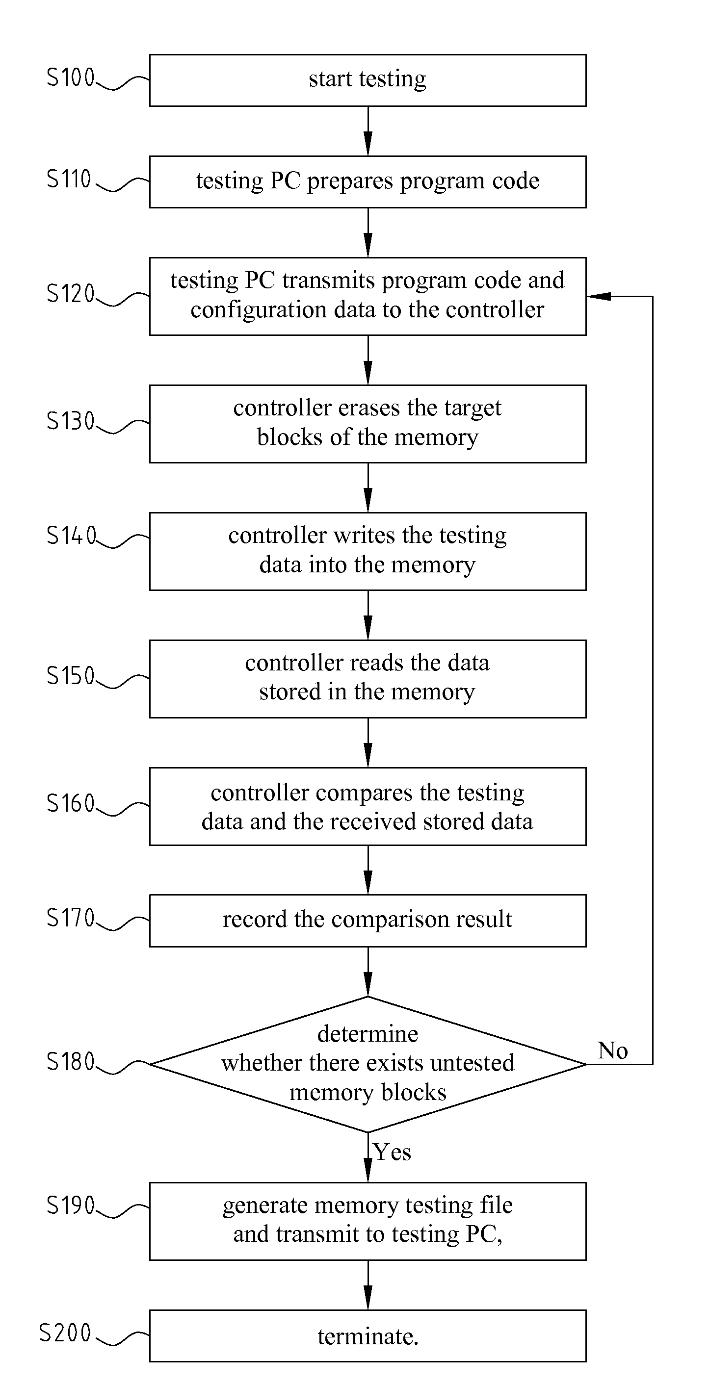
[0013]It is worth noting that in the low level comparison process, an algorithm is used to generate different data for different memory addresses for writing, read and comparison. The present invention does not use fixed data for flash memory testing; instead, the present invention uses the comparison provided by the testing PC. Compared with the conventional testing mode, the present invention provides both the accuracy of the low level comparison and the efficiency of high level comparison. The advantage of the present invention is to accomplish the complicated scanning testing with minimum load of CPU, minimum data transmission and shorter testing time.

Problems solved by technology

Therefore, finding a balance between the correctness of testing and the scanning efficiency is an important issue.
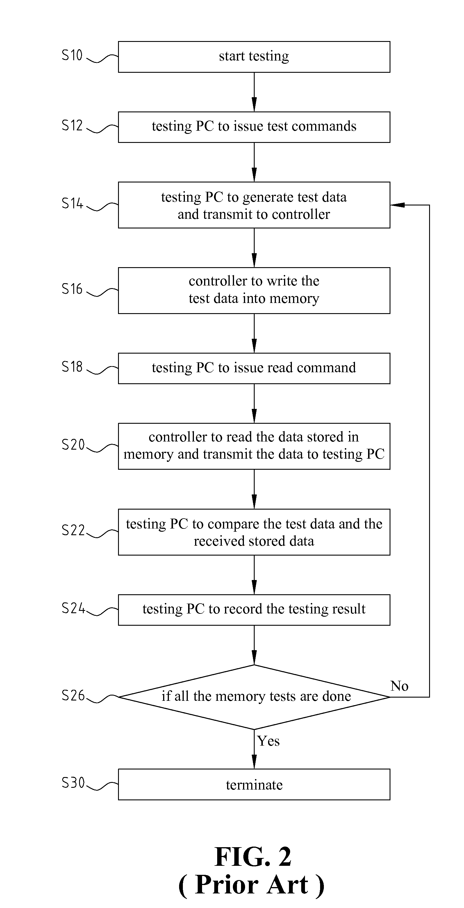
However, the disadvantage of using low-level comparison approach for memory scanning testing is that the CPU of the testing PC usually stays in the state of high load and frequent memory access.
However, while the high level comparison method relies entirely on the testing PC and is suitable for developing efficient testing programs, the high level approach cannot achieve the accuracy of the memory block state as the low level approach.
As the memory chip size decreases rapidly in recent years, the circuit is more complicated and requires operating at high frequency.
The stability of the memory dice is a challenge to the semiconductor industry.
If the memory characteristics are not known in advance, the quality of the memory dice may be challenged.
It becomes an important issue to test the memory in a cost-effective and accurate manner.
This is especially important as the complexity, capability and density of flash memory are increasing and the testing uncertainty may also increase as a result.

Method used


Image

  • Method For Testing Memory
  • Method For Testing Memory
  • Method For Testing Memory

Examples


Embodiment Construction

[0020]FIG. 3 shows a schematic view of the memory testing system of the present invention. As shown in FIG. 3, memory testing system 2 includes a testing PC 10 and a testing board 50, where testing board 50 further includes a controller 51 and a memory 60 to be tested. Controller 51 includes an interface circuit 52, an MCU 54, a RAM 55, a ROM 56 and a logic circuit 58. Interface circuit 52 is for receiving data from testing PC 10 or transmitting data to testing data 10. MCU 54 controls the entire process of controller 51. RAM 55 provides storage for data access. Logic circuit 58 is for processing accesses to memory 60. ROM 56 is for storing the program code compiled by testing PC 10, including algorithm for generating test data, data comparison processing and recording test result.

[0021]FIG. 4 shows a flowchart of a memory testing method of the present invention. As shown in FIG. 4, the memory testing process of the present invention starts with step S100 and proceeds to step S110. ...


PUM


Abstract

A memory testing method is provided, by using the computation capability of a controller to receive the testing command the program code of a testing PC to generate random data or use an algorithm to generate testing data of specific format. Then, the method writes the data directly to the flash memory and read the data from the memory again to compare with the original data. The comparison result is transmitted back to the testing PC. The method greatly reduces the memory access frequency and I / O load of the testing PC so as to improve the testing efficiency.

Description

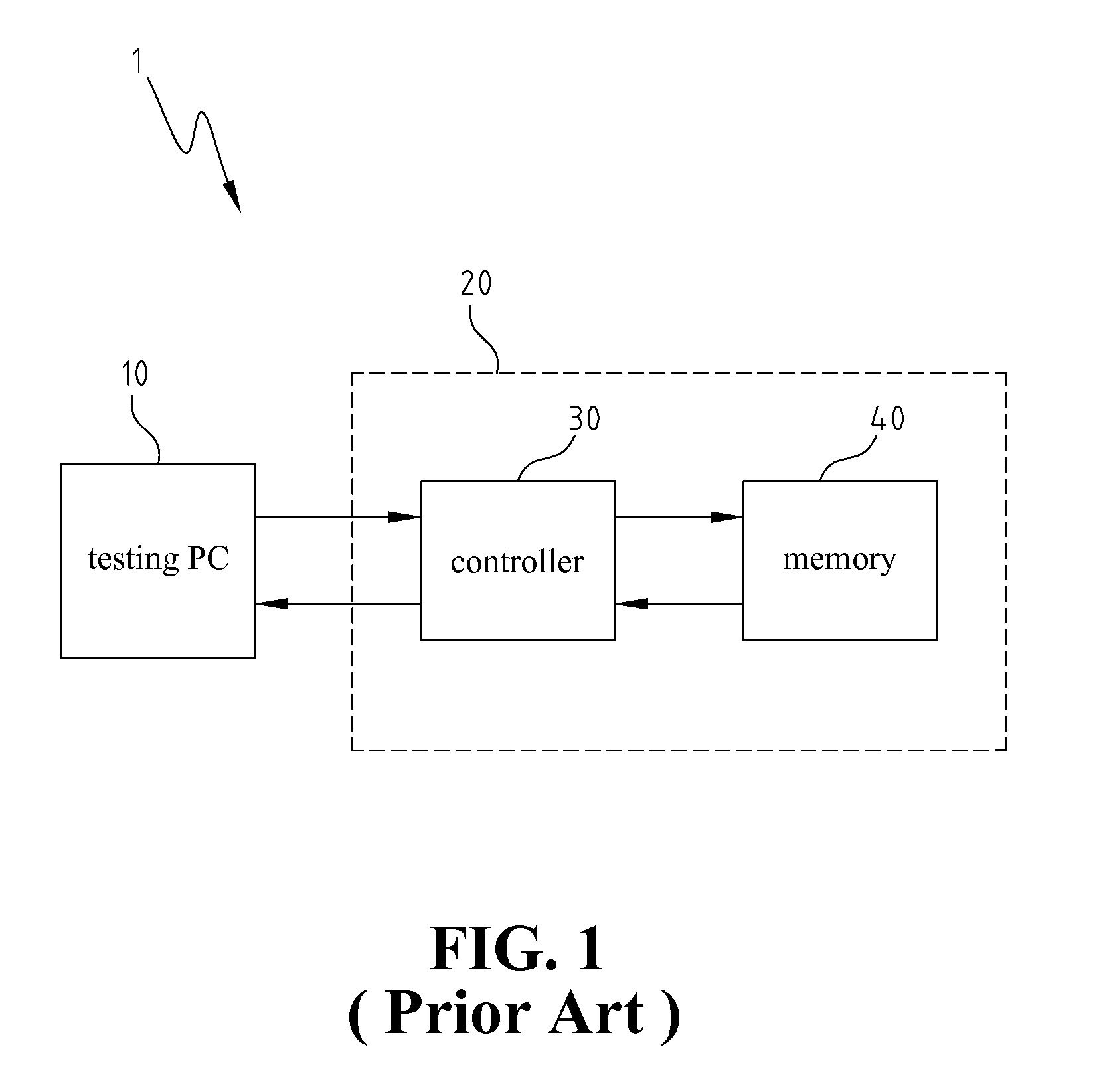
FIELD OF THE INVENTION[0001]The present invention generally relates to a method for testing memory, and more specifically to a method using built-in controller with testing capability for testing memory.BACKGROUND OF THE INVENTION[0002]Flash memory is the most popular storage media in the market, and is widely applied to embedded systems. Flash memory is a solid state, no volatile, rewritable memory, with the operation similar to a hybrid of RAM and harddisk. Like DRAM, flash memory stores the data bits in the memory units. However, the data remains in the memory even when the power is off. With the advantages of high speed, durability, and low voltage requirements, flash memory is suitable for a wide range of devices, such as digital camera, cell phone, printer, palm PC, pager and audio recorder.[0003]FIG. 1 shows a schematic view of c conventional memory testing system. As shown in FIG. 1, memory testing system 1 includes a testing PC 10 and a sorting board 20, where testing PC 10...

Claims


Application Information

Patent Timeline
Patent Type & Authority Applications(United States)
IPC IPC(8): G11C29/04G06F11/22
CPCG11C29/56004G11C29/56
Inventor CHEN, BEI-CHUANCHAN, LI-HSIANGHUANG, SHIH-KAI
Owner MOAI ELECTRONICS
Learn More