Flexible diode package and method of manufacturing

a diode and flexible technology, applied in the field of integrated circuits, can solve the problems of limited life cycle, reduced manufacturing efficiency, and limited thermal cycling capability of solder joints in this design, and achieve the effects of reducing production costs, reducing manufacturing costs, and simplifying packaging

Inactive Publication Date: 2010-06-03
MICROSEMI
View PDF1 Cites 30 Cited by
  • Summary
  • Abstract
  • Description
  • Claims
  • Application Information

AI Technical Summary

Benefits of technology

[0005]The present invention achieves technical advantages as a single step packaging process that both melts a solder and also cures an adhesive about a microelectronic circuit. The process finds technical advantages by simplifying packaging of a die that may be coupled to a planar flexible lead, which leads to a lower production cost and quicker manufacturing time. The planar flexible lead may be adapted to bend and flex during mechanical stress and during extreme temperature cycling, and allow direct mounting of the device to a member by easily welding or soldering. The invention may comprise a flexible solar cell diode that can be closely positioned on solar panels at an extremely low cost.

Problems solved by technology

As the popularity of solar panels continues to grow, expensive failures have been occurring at an ever increasing rate due to the prolonged effects of thermal expansion and the limited life cycles of solar panel components.
These rigid axial leads can tolerate extreme thermal cycling for a period of time, but have a limited life cycle, and were designed for solder attachment to the solar panel.
The solder joint in this design has limited thermal cycling capability due to thermal expansion mismatch, solder re-crystallization, and solder creep.

Method used


Image

  • Flexible diode package and method of manufacturing
  • Flexible diode package and method of manufacturing
  • Flexible diode package and method of manufacturing

Examples


Embodiment Construction

[0016]The numerous innovative teachings and aspects of the present invention will be described with particular reference to the following exemplary embodiments. However, it should be understood that this class of embodiments provides only a few examples of the many advantageous uses and innovative teachings of the inventor. In general, statements made in the specification of the present application do not necessarily delimit any of the various claimed inventions. Moreover, some statements may apply to some inventive features, but not to others.

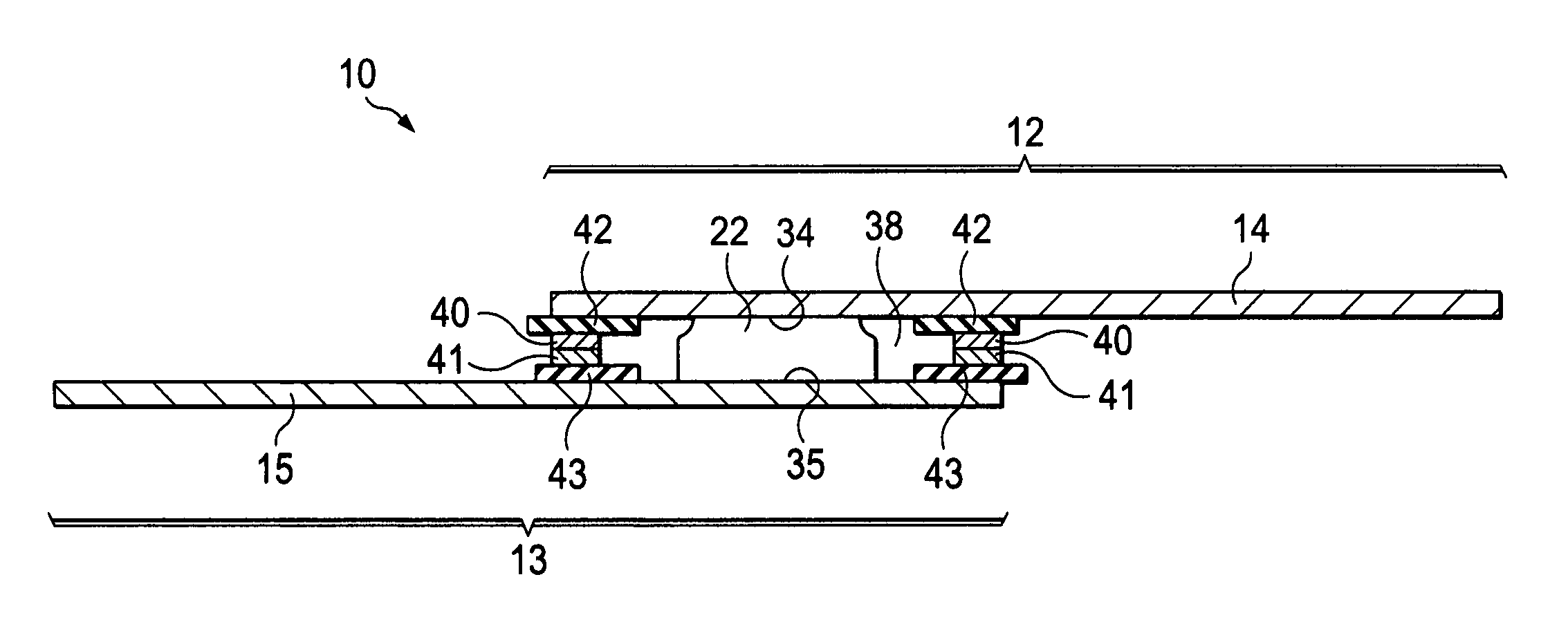
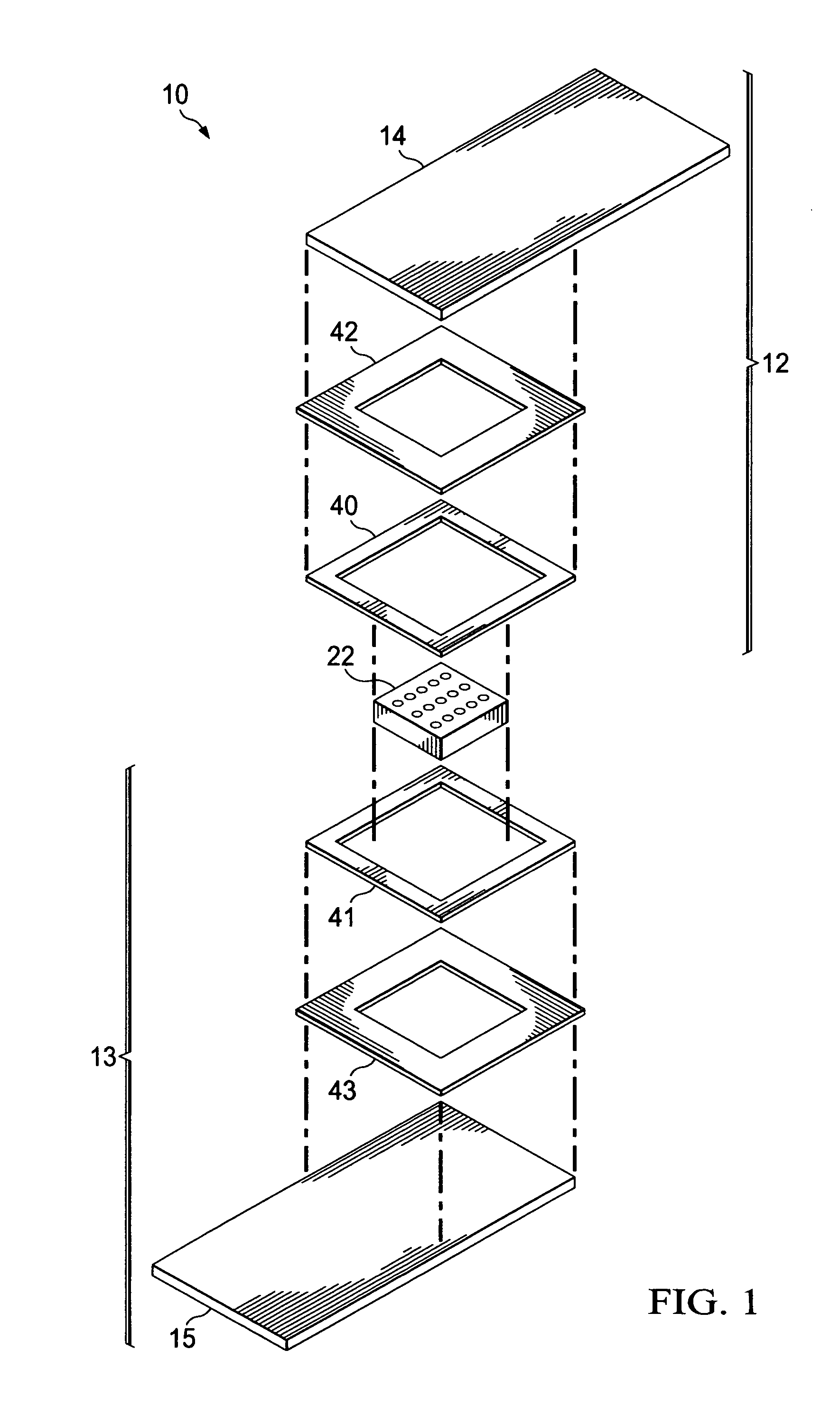
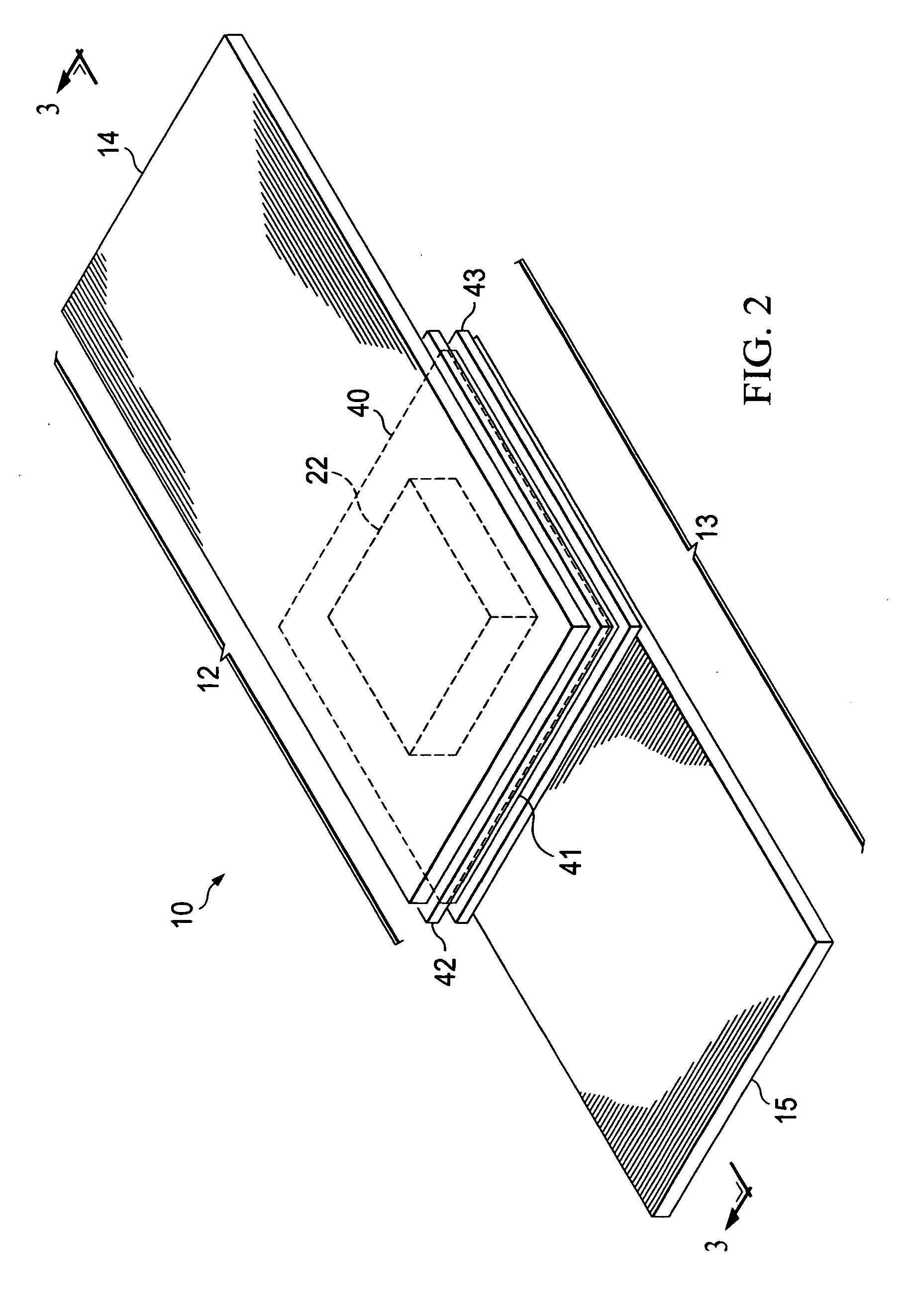
[0017]Microelectronic devices are typically comprised of an integrated circuit diode die encompassed in a package having a plurality of external leads permitting electrical attachment to a printed circuit board. These microelectronic devices are available as commercial devices, and some are available as high reliability devices such as used in military applications, including those integrated in space environments, such as satellites, space ve...


PUM


Abstract

A single step packaging process that both melts a solder and also cures an adhesive about a microelectronic circuit. The process finds technical advantages by simplifying packaging of a die that may be coupled to a planar flexible lead, which leads to a lower production cost and quicker manufacturing time. The planar flexible lead may be adapted to bend and flex during mechanical stress and during extreme temperature cycling, and allow direct mounting of the device to a member by easily welding or soldering. The invention may comprise a flexible solar cell diode that can be closely positioned on solar panels at an extremely low cost.

Description

PRIORITY CLAIM[0001]This application claims priority of U.S. Provisional Patent Application Ser. No. 61 / 197,456 Entitled Flexible Diode Package and Method of Manufacturing, and is a Continuation-in-Part of U.S. patent application Ser. No. 12 / 315,741 entitled “Improved Integrated Circuit with Flexible Planer Leads” filed Dec. 5, 2008 which is a Continuation-in-Part of U.S. patent application Ser. No. 11 / 728,624, entitled “Integrated Circuit with Flexible Planar Leads” filed Mar. 27, 2007, which claims priority of U.S. Provisional Patent Application Ser. No. 60 / 197,456 entitled “Flexible Diode Package and Method of Manufacturing” filed Oct. 27, 2008 and U.S. Provisional Patent Application Ser. No. 60 / 919,794 entitled “Integrated Circuit with Flexible Planar Leads” filed Mar. 23, 2007.FIELD OF THE INVENTION[0002]The present invention is generally directed to integrated circuits, and more particularly to integrated circuit packages and methods of manufacture including diodes that are ad...

Claims


Application Information

Patent Timeline
Patent Type & Authority Applications(United States)
IPC IPC(8): H01L21/60
CPCH01L23/051H01L23/10H01L2924/10253H01L2924/01075H01L2924/01033H01L23/492H01L24/27H01L24/33H01L31/02008H01L2224/73253H01L2924/01029H01L2924/01047H01L2924/01079H01L2924/01082H01L2924/14Y02E10/50H01L2924/01005H01L2924/01006H01L2924/3512H01L2924/00H01L2924/12032
Inventor AUTRY, TRACY
Owner MICROSEMI
Why Eureka
Try Eureka