Organic optoelectronic component

Inactive Publication Date: 2010-06-10
NATIONAL CHIAO TUNG UNIVERSITY
View PDF4 Cites 8 Cited by
  • Summary
  • Abstract
  • Description
  • Claims
  • Application Information

AI Technical Summary

Benefits of technology

[0018]The present invention combines the optoelectronic property of the organic molecule and the film-formation property of the polymer, provides the manuf

Problems solved by technology

When the polymers themselves are used for carrier transfer, for example, or even as active layers, it is difficult to control performance of the components due to the complicated structures of the polymers.
Furthermore, an active layer composed of a polymer and a small molecule is disclosed in Advanced Functional Materials,

Method used


Image

  • Organic optoelectronic component
  • Organic optoelectronic component
  • Organic optoelectronic component

Examples


Example

EXAMPLE 1

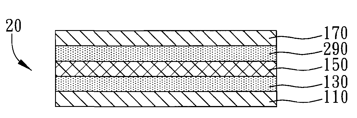
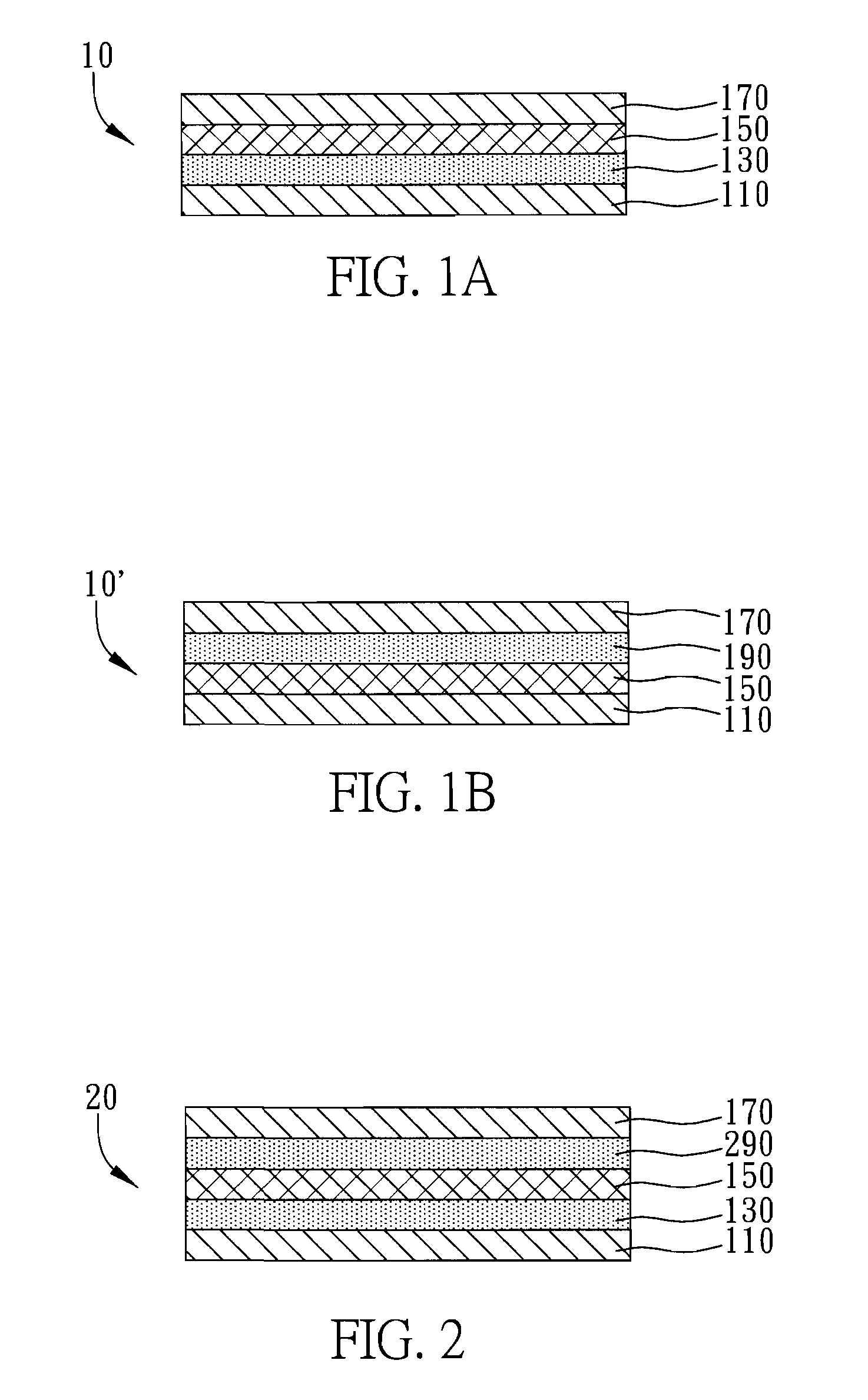
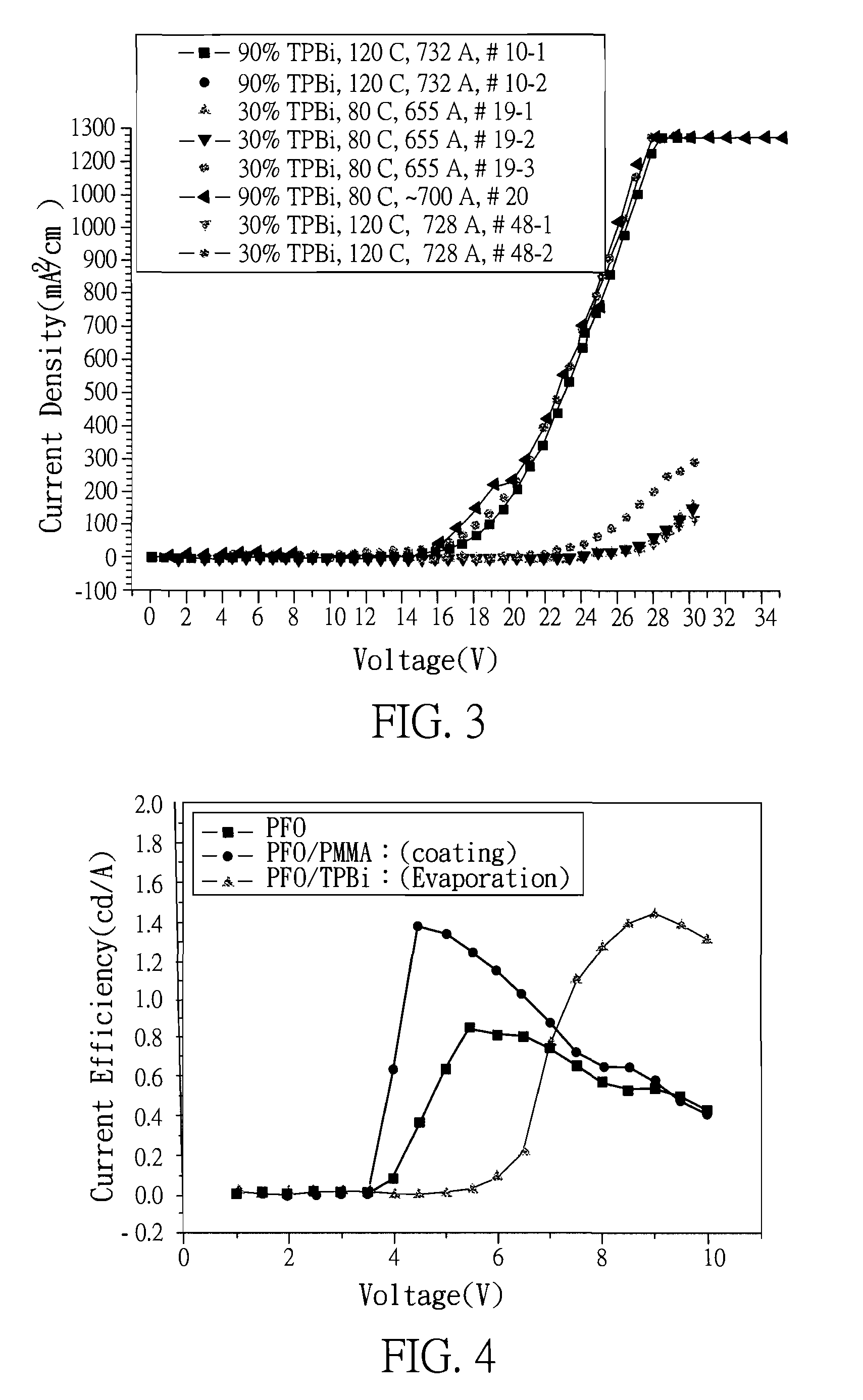
[0046]In the first example of the present invention, the first electrode is an anode, the organic molecule as the hole blocking material and the second intermediate layer is 1,3,5-tris(N-phenylbenzimidazol-2-yl)benzene (TPBi), the polymer used in the second intermediate layer is poly(methyl methacrylate) (PMMA) with a number average molecular weight of about 1,000,000, the active layer is formed of poly(9,9-dioctylfluorene) (PFO), and the second electrode is a cathode. The fabrication is performed as follows:

[0047]After indium tin oxide (ITO) with a thickness of 150 nm was formed on a glass substrate with a thickness of 0.7 nm as a first electrode (anode), PFO with a thickness of 80 nm was evaporated on the first electrode by thermal evaporation as an active layer or other polymer materials can be selected to form thin films by a solution process as active layers. Then, 30 mg of PMMA and 70 mg of TPBi were dissolved in toluene respectively, and a second mixture containing P...

Example

COMPARATIVE EXAMPLE 1

[0048]The method of Example 1 was repeated, but the second intermediate layer was formed by evaporating TPBi only on the active layer.

[0049]After ITO with a thickness of 150 nm was formed on a glass substrate with a thickness of 0.7 nm as a first electrode (anode), poly(9,9-dioctylfluorene) with a thickness of 60 nm was spin coated on the first electrode by thermal evaporation as an active layer. Then, TPBi was evaporated on the active layer to form the second intermediate layer. Finally, a second electrode (cathode) made of cesium fluoride with a thickness of 2 nm and aluminum with a thickness of 100 nm was formed by thermal evaporation.

[0050]As shown in FIG. 4, a light-emitting component of the present invention including a polymer and an organic molecule has the current efficiency equivalent to that of an component of Comparative Example 1 having a hole blocking layer formed by evaporation. Furthermore, the light-emitting component of Example 1 of the present...

Example

EXAMPLE 2

[0051]The method of Example 1 was repeated, but the organic molecule of the second intermediate layer was 2-(4-biphenylyl)-5-(4-tert-butylphenyl)-1,3,4-oxadiazole (PBD) as a hole blocking material, the polymer of the second intermediate layer is polyvinylpyrrolidone (PVP) with a number average molecular weight of 360,000, and polyfluorene (PFO) was used as a material for the active layer.

[0052]After ITO with a thickness of 150 nm was formed on a glass substrate with a thickness of 0.7 nm as a first electrode (anode), PFO with a thickness of 60 nm was coated on the first electrode by spin coating as an active layer or other polymer materials can be selected to form thin films by a solution process as active layers. Then, 50 mg of PVP and 50 mg of PBD were dissolved in 10 ml of n-butanol respectively, and a second mixture containing PVP and PBD was coated on the active layer by spin coating. The active layer would not be damaged by the second mixture since the material of the...


PUM

PropertyMeasurementUnit
Number average molecular weightaaaaaaaaaa
Molecular weightaaaaaaaaaa

Abstract

An organic optoelectronic component is provided, which includes a first electrode, an active layer formed on the first electrode, a second intermediate layer formed on the active layer, and a second electrode formed on the second intermediate layer, wherein the second intermediate layer is formed with a second mixture containing a second polymer and at least a second organic molecule. The second organic molecule is one for forming hole transferring material, electron transferring material, electron blocking material or hole blocking material. The organic optoelectronic component of the present invention is prepared by a solution process, thereby simplifying the process, improving film-formation property, and enhancing component efficiency.

Description

FIELD OF THE INVENTION[0001]The invention relates to an organic optoelectronic component, more particularly, to an organic optoelectronic component having an intermediate layer having a mixture of a polymer and an organic molecule.BACKGROUND OF THE INVENTION[0002]Optoelectronic components, such as light-emitting diodes, solar cells and light sensors, generate electromagnetic radiation or current, according to their optical properties or electronic properties.[0003]For example, organic light sensors convert optical signals into electric signals by photosensitive components. Specifically, organic photosensitive materials in the organic light sensors absorb electromagnetic radiation to produce an excited molecular state, which is excitons having electron-hole pairs, and the so-called optoelectronic current is generated when the electron-hole pairs are separated.[0004]Generally, layers with different functions are desired to facilitate carrier transfer or carrier block in order to achie...

Claims


Application Information

Patent Timeline
IPC IPC(8): H01L29/08H01L51/40
CPCC08G2261/3142C08G2261/5222Y02E10/549Y02P70/50H10K85/111H10K85/115H10K50/14H10K2102/103H05B33/20H05B33/14H10K50/00
Inventor MENG, HSIN-FEIHORNG, SHENG-FUTSENG, HSIN-RONGLI, GUAN-CHENG
Owner NATIONAL CHIAO TUNG UNIVERSITY
Why Eureka
Try Eureka