Semiconductor memory device and semiconductor memory system storing multilevel data

a semiconductor memory and memory device technology, applied in static storage, digital storage, instruments, etc., can solve the problems of reducing the writing performance and not greatly different time required to write data in the 2-level block

Active Publication Date: 2010-06-10
KIOXIA CORP
View PDF6 Cites 22 Cited by
  • Summary
  • Abstract
  • Description
  • Claims
  • Application Information

AI Technical Summary

Benefits of technology

[0012]According to a first aspect of the invention, there is provided a semiconductor memory device comprising: a first memory cell configured to store data of k bits (k is a natural number of 2 or more); and a second memory cell configured to store data of h bits (h<k); wherein the first memory cell stores data of i bits (i<=K), and the second memory cell stores data of h bits (h<i) generated from the data of i bits.

Problems solved by technology

Therefore, there is a problem that a threshold level of a cell in which data has been written in the first place fluctuates with writing in an adjacent cell.
However, when writing 2 bits (4 levels) in 1 cell, a time required to write data in the 2-level block is not greatly different from a time required to write data in a four-level block.
Therefore, an increase in writing in the 2-level block is relatively large, thereby resulting in a problem that writing performance is degraded.

Method used


Image

  • Semiconductor memory device and semiconductor memory system storing multilevel data
  • Semiconductor memory device and semiconductor memory system storing multilevel data
  • Semiconductor memory device and semiconductor memory system storing multilevel data

Examples


first embodiment

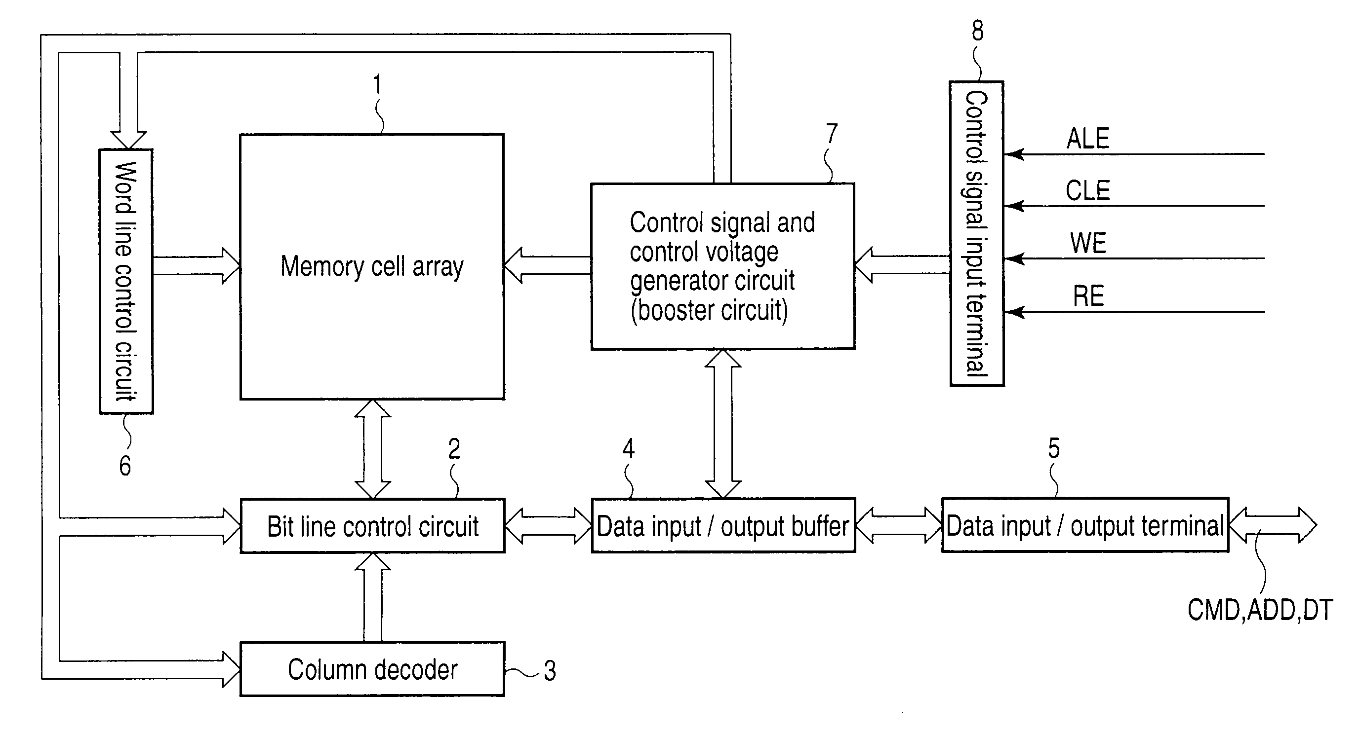
[0054]FIG. 1 shows a NAND flash memory as a semiconductor memory device that stores 2 levels (one bit) or 4 levels (2 bits) in a memory cell.

[0055]A memory cell array 1 includes a plurality of bit lines, a plurality of word lines, and a common source line, and memory cells in which data can be electrically rewritten and which are made up of, for example, EEPROM cells are arranged in a matrix. A bit line control circuit 2 for controlling bit lines and a word line control circuit 6 are connected to the memory cell array 1.

[0056]The bit line control circuit 2 reads the data in a memory cell of the memory cell array 1 via a bit line, detects the state of a memory cell of the memory cell array 1 via a bit line, or writes data into a memory cell of the memory cell array 1 by applying a write control voltage to the memory cell via a bit line. A column decoder 3 and a data input / output buffer 4 are connected to the bit line control circuit 2. A data storage circuit in the bit line control c...

second embodiment

[0174]FIG. 21 shows a write sequence according to a second embodiment. In the first embodiment, reading and restoration of 4-level data are executed after writing in the block SLB in an adjacent cell. On the other hand, in the second embodiment, reading and restoration of 4-level data are carried out before rough writing of 4-level data with respect to an adjacent cell. Since reading 4-level data is effected before writing in an adjacent cell, the 4-level data is not affected by capacitance coupling due to writing in the adjacent cell. Therefore, a threshold distribution is shifted as shown in FIG. 13 (3) to widen a read margin. However, in this case, read 2-level data must be held. Accordingly, in the data control unit 10b shown in FIG. 8, two more data latch circuits must be additionally provided. That is, the data latch circuits are ADL, BDL, and XDL in the first embodiment, but circuits CDL and DDL are further required.

[0175]A flow of a (program) in this example is as follows.[0...

third embodiment

[0184]FIGS. 22 and 23 show a third embodiment. In the first and second embodiments, 4-level data is roughly written in a memory cell of the block MLB, and then 2-level data is written in a memory cell of the block SLB. On the other hand, a third embodiment is characterized in that 2-level data is first written into a memory cell of the block SLB, and then 4-level data is roughly written in a memory cell of the block MLB. In the third embodiment, a write operation is the same as those in the first and second embodiments, thereby omitting a description thereof.

[0185]The third embodiment can also obtain the same effect as those in the first and second embodiments.

[0186]FIG. 24 shows a modification of the third embodiment. When generating data obtained by subjecting data corresponding to two pages to exclusive NOR in a controller, the controller first supplies an address of the block SLB and data of exclusive NOR to a NAND flash memory. Thereafter, writing in the block SLB is first carr...


PUM


Abstract

A first memory cell stores data of k bits in one cell. A second memory cell stores data of h bits (h<k) in one cell. Data of i bits (i<=k) is stored in the first memory cell, and data of h bits (h<i) generated from the i-bit data is stored in the second memory cell.

Description

CROSS-REFERENCE TO RELATED APPLICATIONS[0001]This application is based upon and claims the benefit of priority from prior Japanese Patent Application No. 2008-313559, filed Dec. 9, 2008, the entire contents of which are incorporated herein by reference.BACKGROUND OF THE INVENTION[0002]1. Field of the Invention[0003]The present invention relates to, e.g., a NAND flash memory, and to a semiconductor memory device and a semiconductor memory system that can store multilevel data.[0004]2. Description of the Related Art[0005]In a NAND flash memory, all or half of cells aligned in a row direction are connected with each of the writing or reading latch circuits through each of the bit lines. A write operation or a read operation is collectively carried out with respect to all or half of the cells (e.g., 2 to 8 kB cells) aligned in the row direction.[0006]A write or read unit is called a page, and a plurality of pages constitute a block. Data in the memory cells are erased in units of blocks...

Claims


Application Information

Patent Timeline
Patent Type & Authority Applications(United States)
IPC IPC(8): G11C16/04
CPCG11C16/10G11C16/04
Inventor SHIBATA, NOBORU
Owner KIOXIA CORP
Why Eureka
Try Eureka