Bipolar electrostatic chuck

a bipolar electrostatic and chuck technology, applied in the direction of electrostatic holding devices, basic electric elements, electric devices, etc., can solve the problems of deterioration of dielectric breakdown strength between adjacent electrodes, discharge limit, voids, etc., and achieve excellent attracting performance, excellent flatness of held samples, and shorten the distance between the first electrode and the second electrode

Active Publication Date: 2010-06-17
CREATIVE TECH CORP
View PDF17 Cites 36 Cited by
  • Summary
  • Abstract
  • Description
  • Claims
  • Application Information

AI Technical Summary

Benefits of technology

[0058]The bipolar electrostatic chuck according to the present invention is structured to have the first electrode, the interelectrode insulating layer, and the second electrode in the order of distance from the sample attracting plane in the depth direction of the insulating material. With the above structure, the bipolar electrostatic chuck according to the present invention is excellent in electrical insulation, and is capable of shortening the distance between the first electrode and the second electrode as much as possible, thereby exercising the excellent attracting performance. As a result, the bipolar electrostatic chuck according to the present invention is excellent in the flatness of the held sample, and exercises the sufficient attracting performance with respect to a glass substrate that exceeds 1 m×1 m so as to accept the recent large size glass substrate, a silicon wafer that is equal to or more than 300 mm in diameter, or the like. Also, the bipolar electrostatic chuck according to the present invention is capable of exercising the excellent attracting performance. As a result, the bipolar electrostatic chuck according to the present invention is capable of conducting in the low voltage operation, is advantageous in the economical viewpoint, eliminates the discharge problem as much as possible, and is high in the reliability.
[0059]In addition, the bipolar electrostatic chuck according to the present invention reduces an area in which the first electrode and the second electrode are overlapped with each other when the sample attracting plane is viewed in the depth direction as much as possible, thereby making it possible to reduce the capacitance of the electrostatic chuck, and also making it possible to eliminate the difficulty of dismounting the sample from the sample attracting plane after turning off the voltage that has been applied to both of the electrodes. Further, in the case where an electrically conductive layer is formed on the surface of the insulating material, and the surface of the electrically conductive layer serves as the sample attracting plane, the bipolar electrostatic chuck according to the present invention is capable of reducing the time constant of the electrostatic chuck regardless of the area in which the first electrode and the second electrode are overlapped with each other in the normal line direction of the sample attracting plane. The bipolar electrostatic chuck according to the present invention is also capable of eliminating the difficulty of dismounting the sample from the sample attracting plane after a voltage has been applied to both of the electrodes.

Problems solved by technology

However, in the case where the distance between the electrodes that are adjacent to each other is shortened, there arises a problem of a discharge limit.
Also, voids occur when an adhesive agent for forming an adhesive layer that fixes the respective insulating layers to each other or the insulating layers with the electrodes is bonded.
As a result, the dielectric breakdown strength is remarkably deteriorated between the adjacent electrodes.
For that reason, in the conventional bipolar electrostatic chuck that narrows the interval between the electrodes as described above, a voltage that can be actually applied is limited, and there arises such a problem that a sufficient attracting performance, i.e., gradient force, cannot be exercised because a weight per unit area is increased with respect to a semiconductor wafer that is increasingly enlarged diameter in size or a glass substrate that is used for a liquid crystal TV or a flat panel display which are increasingly enlarged in size.
On the other hand, in the case where an insulating sample is attracted by the electrostatic chuck, there arises such a problem that a sample is difficult to dismount from the attracting plane of the sample due to the residual charges even if a voltage that is applied to the electrodes is turned off.
In particular, this problem becomes severe as the sample is increasingly enlarged in size.

Method used


Image

  • Bipolar electrostatic chuck
  • Bipolar electrostatic chuck
  • Bipolar electrostatic chuck

Examples


first embodiment

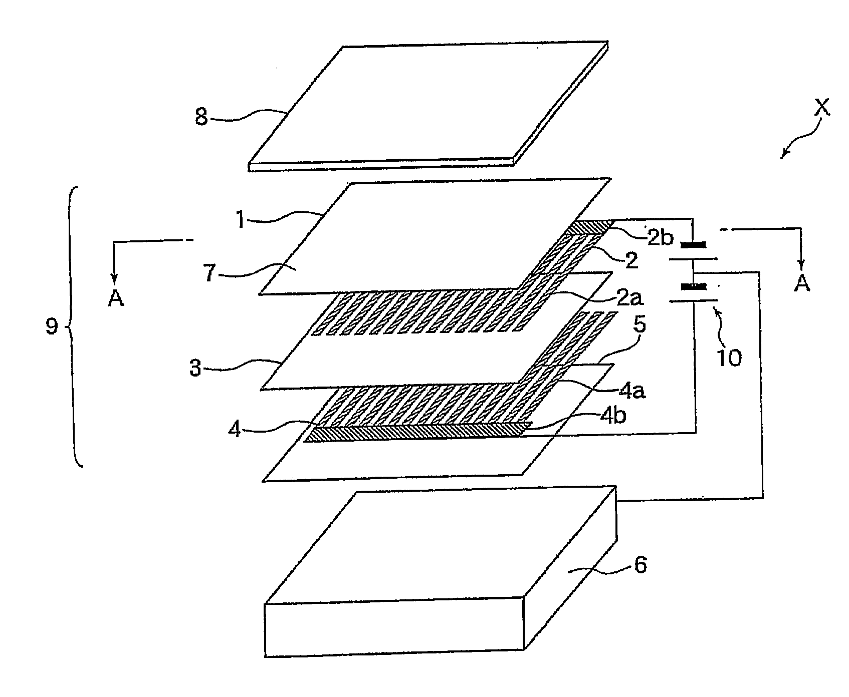
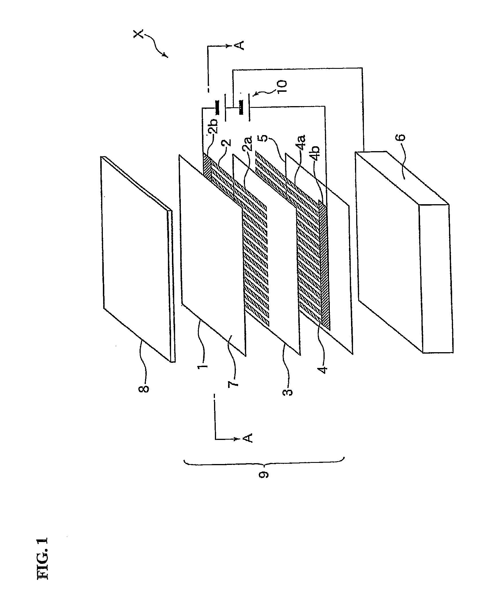
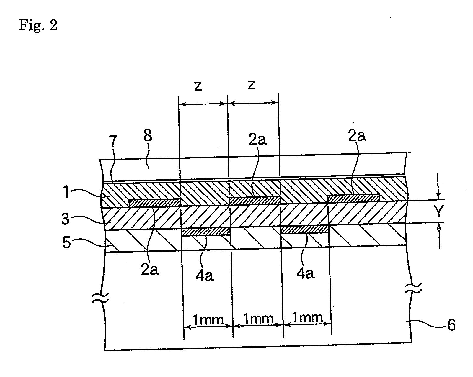
[0090]FIG. 1 shows an explanatory exploded perspective view of a bipolar electrostatic chuck X according to a first embodiment of the present invention. The bipolar electrostatic chuck X includes an upper insulating layer 1 that is formed of a polyimide film having a thermoplastic polyimide film on a lower surface thereof which is 100 mm in height×100 mm in width, 50 μm in thickness, and a dielectric constant ε=3.5, a first electrode 2 made of copper which is 3 μm in thickness, and an interelectrode insulating layer 3 that is formed of a polyimide film which is 100 mm in height×100 mm in width, 50 μm in thickness, and a dielectric constant ε=3.5. The bipolar electrostatic chuck X also includes a second electrode 4 made of copper that is 3 μm in thickness, a lower insulating layer 5 that is formed of a polyimide film having a thermoplastic polyimide film on an upper surface thereof which is 100 mm in height×100 mm in width, 50 μm in thickness, and a dielectric constant ε=3.5, and a m...

second embodiment

[0097]FIG. 4 shows an explanatory cross-sectional view of a bipolar electrostatic chuck X according to a second embodiment of the present invention. FIG. 5 shows an explanatory partial plan view of a first electrode 2 and a second electrode 14 of the bipolar electrostatic chuck X according to the second embodiment, viewed in a depth direction of the sample attracting plane 7.

[0098]In the bipolar electrostatic chuck X according to the second embodiment, an electrode width of the band-like portions 14a of the second electrode 14 is set to 0.6 mm, and the band-like portions 14a of the second electrode 14 are arranged in the center of gaps (1 mm) which are formed between the respective band-like portions 2a of the first electrode 2. Band-like comb teeth of the first electrode 2 and band-like comb teeth of the second electrode 14 are alternately arranged, and the first electrode 2 and the second electrode 14 are arranged when the sample attracting plane 7 is viewed in the depth direction...

third embodiment

[0099]FIG. 6 shows an explanatory exploded perspective view of a bipolar electrostatic chuck X according to a third embodiment of the present invention. FIG. 7 shows an explanatory cross-sectional view (a part of a cross-section A-A of FIG. 6) of the bipolar electrostatic chuck X according to the third embodiment. FIG. 8 shows an explanatory partial plan view of a first electrode 2 and a second electrode 24 of the bipolar electrostatic chuck X according to the third embodiment, viewed in a depth direction of the sample attracting plane 7. In FIG. 8, a dotted area portion represents a portion in which the second electrode 24 is overlapped with the first electrode 2 when the sample attracting plane 7 is viewed in the depth direction.

[0100]In the bipolar electrostatic chuck X according to the third embodiment, the conditions other than a condition in which the second electrode 24 is formed in a plane having a planar area that is 80 mm in height×80 mm in width are set to be identical wi...


PUM


Abstract

A bipolar electrostatic chuck which has excellent dielectric breakdown strength and provides excellent attracting performance. The bipolar electrostatic chuck eliminates difficulty in dismounting a sample from a sample attracting plane as much as possible after application of a voltage to electrodes is finished. The bipolar electrostatic chuck is provided with a first electrode and a second electrode in an insulator and permits a surface of the insulator to be the sample attracting plane. The insulator has the first electrode, an interelectrode insulating layer and the second electrode in this order from the sample attracting plane in the depth direction. The second electrode has a region not overlapping with the first electrode in a normal line direction of the sample attracting plane.

Description

[0001]This application is a Divisional of co-pending application Ser. No. 10 / 591,945 filed on Sep. 8, 2006 and for which priority is claimed under 35 U.S.C. §120. Application Ser. No. 10 / 591,945 is the national phase of PCT International Application No. PCT / JP2005 / 004557 filed on Mar. 15, 2005 under 35 U.S.C. §371, and also claims priority under 35 U.S.C. §119(a) on Patent Application Nos. 2004-081432 and 2004-191280 filed in Japan on Mar. 19, 2004 and Jun. 29, 2004, respectively. The entire contents of each of the above-identified applications are hereby incorporated by reference.TECHNICAL FIELD[0002]The present invention relates to a bipolar electrostatic chuck that electro-statically attracts and holds a sample.BACKGROUND ART[0003]There has been widely employed an electrostatic chuck that electro-statically attracts and holds a sample such as a wafer or a glass in a device that is used in a semiconductor manufacturing process required in forming an integrated circuit on a semicon...

Claims


Application Information

Patent Timeline
Patent Type & Authority Applications(United States)
IPC IPC(8): H01L21/683H01L21/68H02N13/00
CPCH02N13/00H01L21/6833H01L21/68H01L21/687
Inventor FUJISAWA, HIROSHIMIYASHITA, KINYA
Owner CREATIVE TECH CORP
Why Eureka
Try Eureka