Semiconductor device and method of manufacturing the same

a semiconductor device and semiconductor technology, applied in semiconductor devices, semiconductor/solid-state device details, electrical apparatus, etc., can solve the problems of increasing resistance and inductance, not suitable for high-speed operations, and increasing mounting area of semiconductor devices, so as to improve the performance of semiconductor devices, the effect of reducing the productivity

Active Publication Date: 2010-06-24
TESSERA ADVANCED TECH
View PDF7 Cites 72 Cited by
  • Summary
  • Abstract
  • Description
  • Claims
  • Application Information

AI Technical Summary

Benefits of technology

[0012]Accordingly, a preferred aim of the present invention is to provide a technique that enhances performance of a semiconductor device, in which a plurality of semiconductor chips are stacked, without deteriorating the productivity.
[0017]More specifically, in a semiconductor device in which a plurality of semiconductor chips are stacked, performance can be enhanced without deteriorating the productivity.

Problems solved by technology

Moreover, a large number of chips can be mounted in the same mounting area.
However, when the chips are mutually connected by bonding wires, the wiring space for once suspending the bonding wires is needed in a chip peripheral region, and thus the mounting area becomes larger than the chip size.
Moreover, there are problems that resistance and inductance are increased as the bonding wires are long and that this is not suitable for high-speed operations.
However, according to further studies carried out by the present inventors about the method of forming the through-electrode described above, it has been found out that the method has below problems.
Given such background, it has been found out that it would be difficult to form the hole portion for the through-electrode only by the back-surface processing.
The difficulty of processing the through-electrode and the need for higher processing techniques are the cause that lowers the productivity of above-mentioned high-performance semiconductor devices.

Method used


Image

  • Semiconductor device and method of manufacturing the same
  • Semiconductor device and method of manufacturing the same
  • Semiconductor device and method of manufacturing the same

Examples


first embodiment

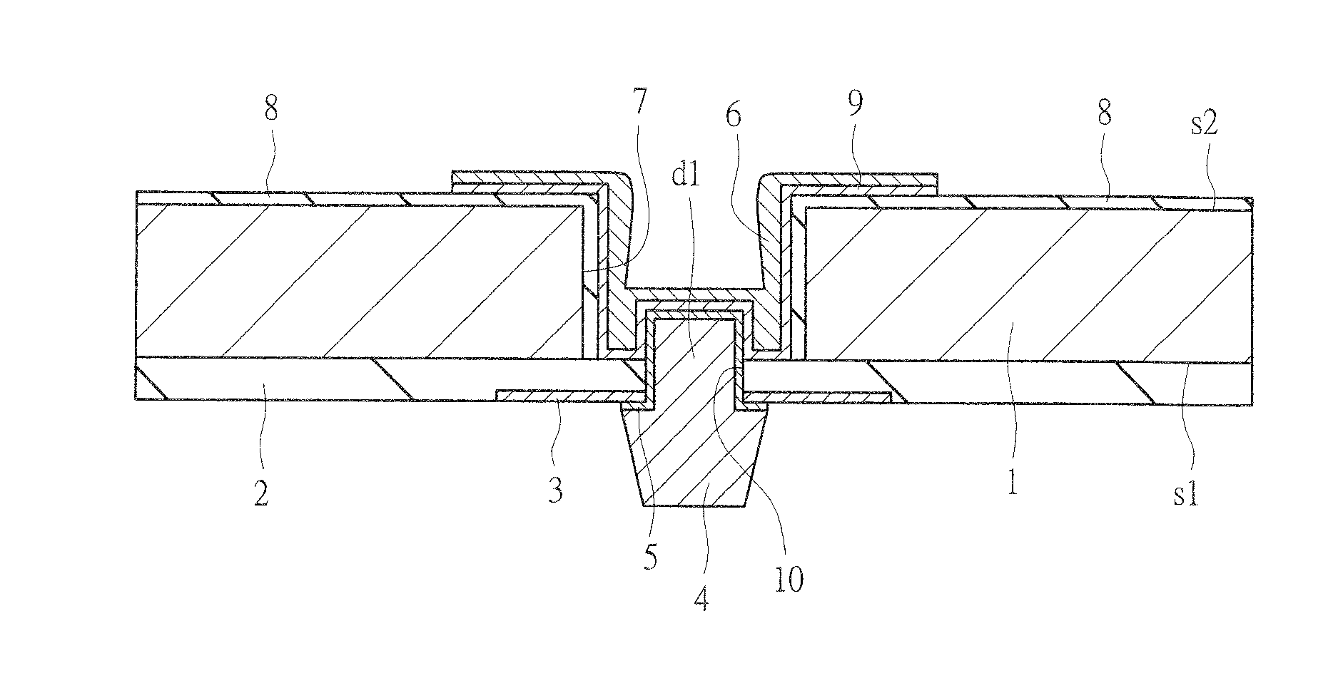
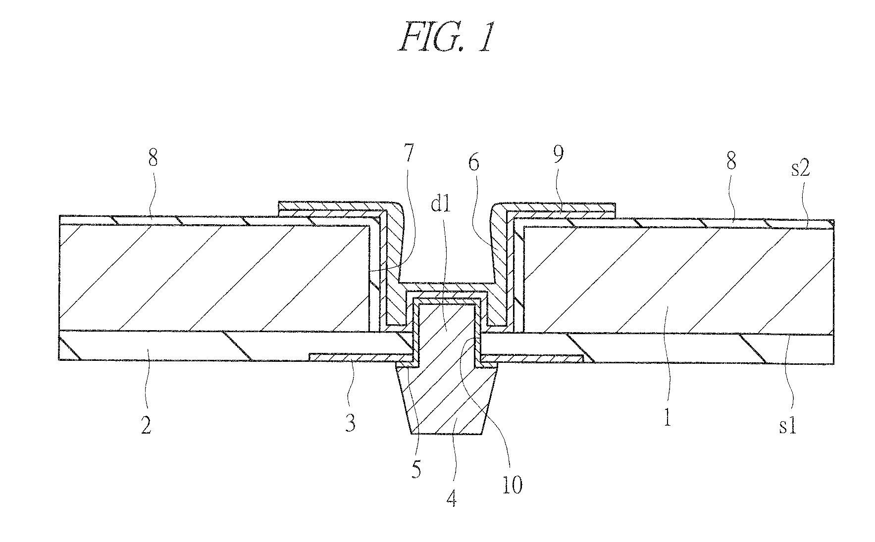
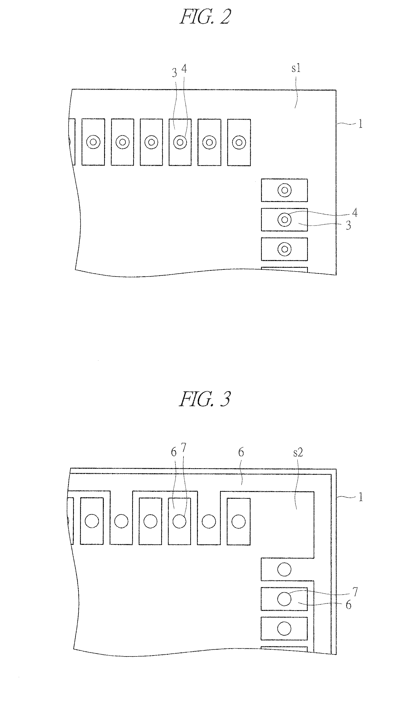
[0074]A configuration of a semiconductor device of a first embodiment will be described with reference to FIGS. 1 to 3. FIG. 1 illustrates a cross-sectional view of a main part of a silicon substrate (semiconductor substrate) 1 which the semiconductor device of the first embodiment has. FIG. 2 illustrates a plan view of a main part of a main surface (first main surface) s1-side of the silicon substrate 1. FIG. 3 illustrates a plan view of a main part of a back surface (second main surface) s2-side of the silicon substrate 1. The main surface s1 and the back surface s2 of the silicon substrate 1 are positioned on the sides opposite to each other in a thickness direction of the silicon substrate 1.

[0075]A plurality of semiconductor elements (elements) such as field effect transistors (FETs), capacitors, and non-volatile memory cells are formed (not illustrated) on the main surface s1 of the silicon substrate 1. Further, an interlayer insulating film 2 is formed on the main surface s1 ...

second embodiment

[0109]In a second embodiment, a structure which exerts different effects by changing the shape of the through-electrode in the semiconductor device of the above-described first embodiment will be described. A semiconductor device of the second embodiment has a similar configuration and similar effects as the semiconductor device of the above-described first embodiment except for the configuration described below.

[0110]A first structure will be described with reference to FIG. 20. The through-electrode of the semiconductor device of the second embodiment has a structure similar to that of the through-electrode of the semiconductor device of the above-described first embodiment. Specifically, the bump electrode 4 formed in the main surface s1-side of the silicon substrate 1 has the protruding portion d1, and the protruding portion d1 penetrates through the pad 3, also penetrates through the interlayer insulating film 2, and protrudes to the inside of the back-surface-electrode hole po...

third embodiment

[0151]A semiconductor device of a third embodiment will be described with reference to FIG. 45. The semiconductor device of the third embodiment has a configuration in which a plurality of semiconductor chips having through-electrodes like those of the above-described first and second embodiments are stacked. Herein, the semiconductor chips are stacked in the manner as described with reference to above-described FIG. 20.

[0152]FIG. 45 illustrates the semiconductor device including the stacked plurality of chips (first chip C1, second chip C2, and third chip C3) having the through-electrodes of the third embodiment. The chips are mutually connected by physical caulking by injecting and pressure-welding the bump electrode 4 formed on an upper-level chip (for example, the second chip C2) into and with the hollow back-surface-electrode hole portions 7 formed in a lower-level chip (for example, the first chip C1). The bump electrodes 4 of the chip of the lowermost layer (in this case, the...


PUM


Abstract

In a semiconductor device in which a plurality of semiconductor chips are stacked, performance is enhanced without deteriorating productivity. The semiconductor device has a plurality of elements, an interlayer insulating film, a pad, and a bump electrode electrically connected with the pad sequentially formed on a main surface of a silicon substrate and has a back-surface electrode formed on a back surface of the silicon substrate and electrically connected with the bump electrode. The bump electrode has a protruding portion penetrating through the pad and protruding toward the silicon substrate side. The back-surface electrode is formed so as to reach the protruding portion of the bump electrode from the back surface side of the silicon substrate toward the main surface side and to cover the inside of a back-surface-electrode hole portion which does not reach the pad, so that the back-surface electrode is electrically connected with the bump electrode.

Description

CROSS-REFERENCE TO RELATED APPLICATION[0001]The present application claims priority from Japanese Patent Application No. JP 2008-323581 filed on Dec. 19, 2008, the content of which is hereby incorporated by reference into this application.TECHNICAL FIELD OF THE INVENTION[0002]The present invention relates to a semiconductor device and techniques of manufacturing the same and, particularly, relates to techniques effectively applied to a semiconductor device having a structure in which a plurality of semiconductor chips are stacked.BACKGROUND OF THE INVENTION[0003]In mobile devices such as mobile phones and digital cameras, SiP (System in Package) in which a plurality of chips are stacked and mounted in a semiconductor package is widely used. When the chips are disposed in the manner that they are stacked, the mounting area can be reduced compared with the case in which they are horizontally disposed. Moreover, a large number of chips can be mounted in the same mounting area. However,...

Claims


Application Information

Patent Timeline
Patent Type & Authority Applications(United States)
IPC IPC(8): H01L23/498H01L21/768
CPCH01L21/6835H01L21/76898H01L2924/0002H01L2924/00014H01L2924/1306H01L2224/0401H01L2224/05572H01L23/481H01L24/11H01L24/12H01L24/16H01L24/81H01L24/94H01L25/0657H01L25/50H01L2221/68372H01L2224/1147H01L2224/11472H01L2224/13009H01L2224/13022H01L2224/13025H01L2224/13099H01L2224/274H01L2224/81136H01L2224/81365H01L2224/81801H01L2225/06513H01L2225/06517H01L2225/06541H01L2924/01002H01L2924/01005H01L2924/01013H01L2924/01018H01L2924/01022H01L2924/01029H01L2924/01074H01L2924/01078H01L2924/01079H01L2924/19041H01L2924/30107H01L2924/01006H01L2924/01024H01L2924/01033H01L2924/014H01L24/27H01L23/5386H01L2924/14H01L2924/1205H01L2924/10253H01L2924/1451H01L2224/13021H01L2224/13014H01L2224/13013H01L24/13H01L2924/01028H01L2224/81345H01L2224/0557H01L2924/00H01L2224/05552H01L2224/06181H01L2224/05557H01L2224/16058H01L2224/16146H01L2224/81898H01L2224/13012H01L2224/16112H01L2924/35121H01L2924/00012H01L23/5226H01L23/528H01L25/074
Inventor KAWASHITA, MICHIHIROYOSHIMURA, YASUHIROTANAKA, NAOTAKANAITO, TAKAHIROAKAZAWA, TAKASHI
Owner TESSERA ADVANCED TECH
Why Eureka
Try Eureka