Filter for plasma display and fabricating method thereof

a technology for plasma displays and filters, applied in the direction of discharge tubes/lamp details, coatings, non-electron-emitting shielding screens, etc., can solve the problems of increasing processing time and cost, and achieve the effects of reducing manufacturing costs, reducing thickness, and restrainting cracks

Inactive Publication Date: 2010-07-01
SAMSUNG SDI CO LTD
View PDF2 Cites 11 Cited by
  • Summary
  • Abstract
  • Description
  • Claims
  • Application Information

AI Technical Summary

Benefits of technology

[0007]Aspects of the present invention provide a filter for a plasma display allowing reduction of thickness so as to achieve a slim plasma d...

Problems solved by technology

However, the addition of the color compensating layer and the an...

Method used


Image

  • Filter for plasma display and fabricating method thereof
  • Filter for plasma display and fabricating method thereof
  • Filter for plasma display and fabricating method thereof

Examples


Embodiment Construction

[0040]Reference will now be made in detail to the present embodiments of the present invention, examples of which are illustrated in the accompanying drawings, wherein like reference numerals refer to the like elements throughout. The embodiments are described below in order to explain the present invention by referring to the figures.

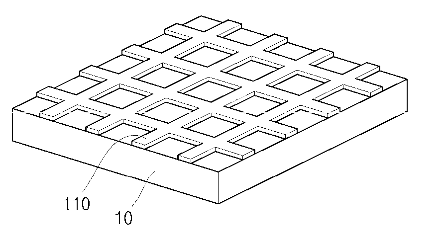
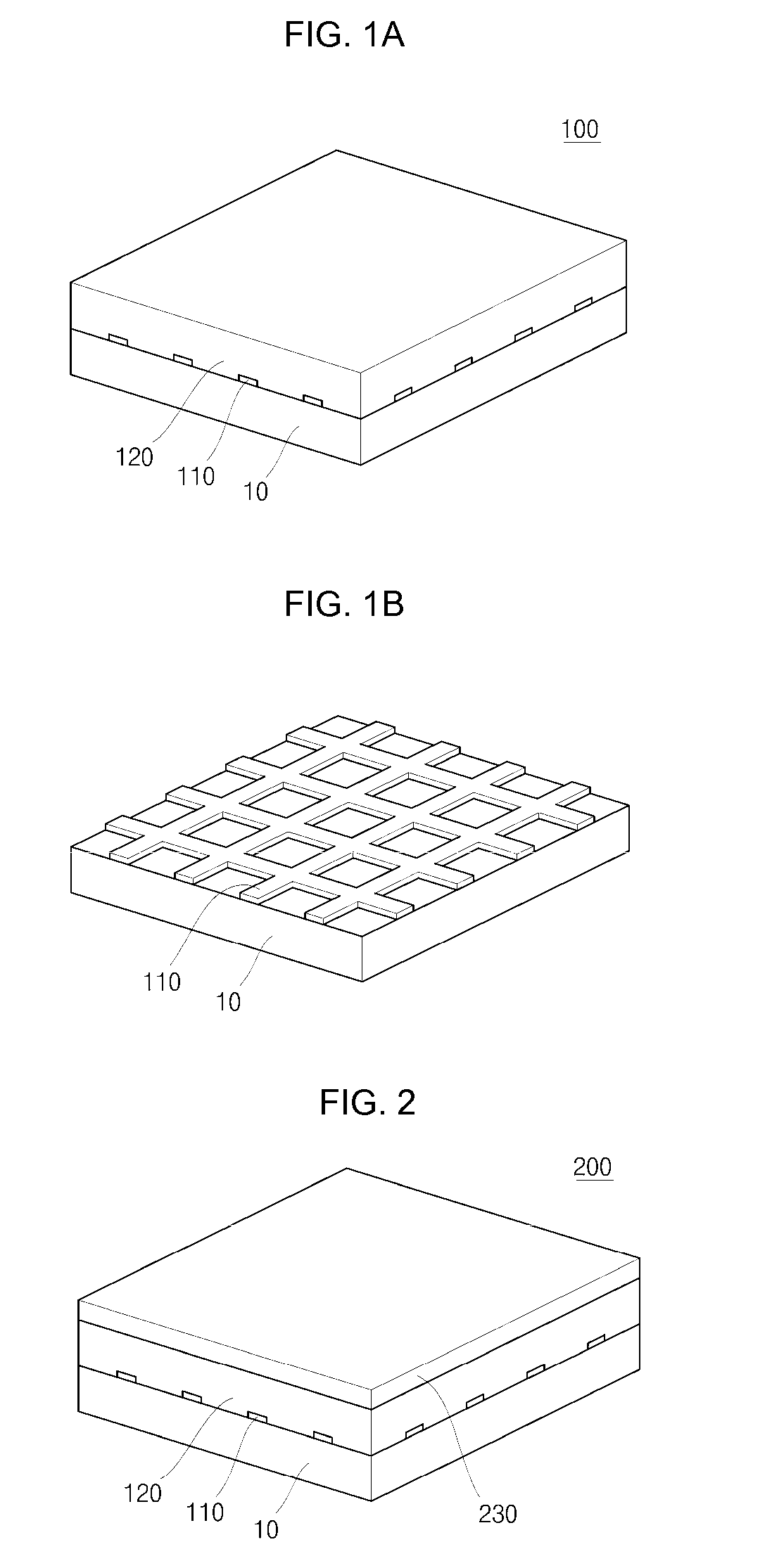
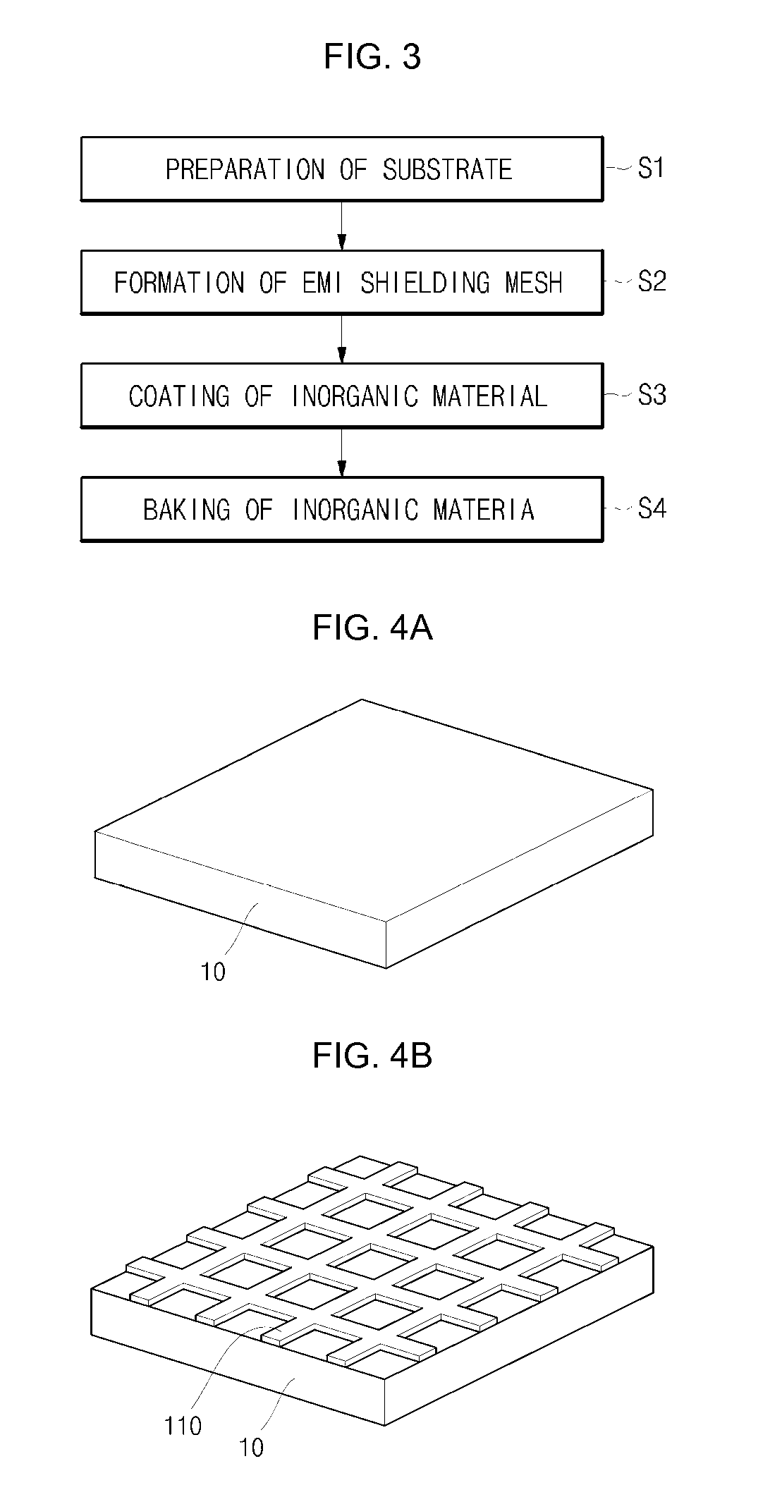
[0041]Hereinafter, a filter 100 of a plasma display according to an embodiment of the present invention will be described. FIG. 1A is a perspective view illustrating the filter 100 and FIG. 1B is a perspective view illustrating an electromagnetic interference shielding mesh 110 applied to the filter 100. In particular, referring to FIGS. 1A and 1B, the filter 100 includes an EMI shielding mesh 110 formed on a substrate 10 and a hard coating layer 120 formed on the EMI shielding mesh 110. Herein, the term “formed on” is used with the same meaning as “located on” or “disposed on” and is not meant to be limiting regarding any particular fabrication proces...


PUM


Abstract

A filter for a plasma display includes an electromagnetic interference shielding mesh formed on a substrate to shield electromagnetic waves and a hard coating layer made of inorganic material formed on the electromagnetic interference shielding mesh. The filter is fabricated so as to provide a reduced thickness of a plasma display, to prevent cracks from being generated on surfaces of the mesh and to reduce manufacturing costs.

Description

CROSS-REFERENCE TO RELATED APPLICATIONS[0001]This application claims the benefit of Korean Patent Application No. 10-2008-0136878 filed on Dec. 30, 2008 in the Korean Intellectual Property Office, the disclosure of which is incorporated herein by reference.BACKGROUND OF THE INVENTION[0002]1. Field of the Invention[0003]Aspects of the present invention relate to a filter for a plasma display and a fabricating method thereof.[0004]2. Description of the Related Art[0005]An electromagnetic interference (EMI) film for a plasma display is typically fabricated in a method by which copper is plated onto or thinly bonded to a substrate of polyethylene terephthalate (PET), which is etched in the form of a mesh, after which the etched copper is oxidized black. However, the mesh lines of the EMI shield film typically have a thickness of about 10 μm and have a wide prominence (that is, the mesh lines prominently protrude from the surface of the substrate).[0006]Since it is difficult to make the ...

Claims


Application Information

Patent Timeline
IPC IPC(8): H01J1/52B05D5/12H05K9/00
CPCH01J11/10H01J11/44H01J2211/444H01J2211/446H05K9/0096G02B5/20H05K9/00
Inventor LEE, JINYOUNGLEE, SUNGYONGPARK, JAEYOUNGKIM, JAEHYUNGKWON, DOHYUKL
Owner SAMSUNG SDI CO LTD
Why Eureka
Try Eureka