Shift register circuit

a technology of shift register and shift register, which is applied in the direction of static storage, digital storage, instruments, etc., can solve the problems of increasing power consumption, and achieve the effect of high driving capacity and low power consumption of clock signals

Active Publication Date: 2010-07-01
TRIVALE TECH
View PDF33 Cites 44 Cited by
  • Summary
  • Abstract
  • Description
  • Claims
  • Application Information

AI Technical Summary

Benefits of technology

[0016]It is the object of the present invention to provide a shift register circuit that achieves a low power consumption in a clock signal and a high driving capacity.

Problems solved by technology

This is one of the reasons that increase power consumption.

Method used


Image

  • Shift register circuit
  • Shift register circuit
  • Shift register circuit

Examples


first embodiment

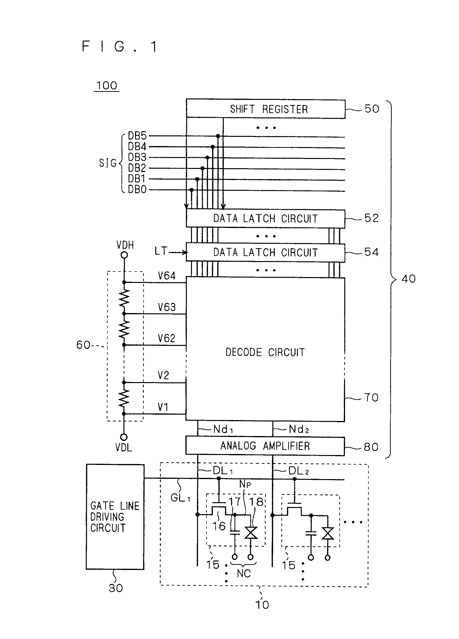
[0050]FIG. 1 is a schematic block diagram showing a configuration of a display apparatus according to the first embodiment of the present invention. In FIG. 1, an entire configuration of a liquid crystal display apparatus 100 is shown as a representative example of the display apparatus. It should be noted that a gate line driving circuit according to the present invention is not limited to application to a liquid crystal display apparatus, and can be widely applied to electro-optic apparatuses such as electroluminescence (EL), organic EL, plasma display, electronic paper, and image sensor.

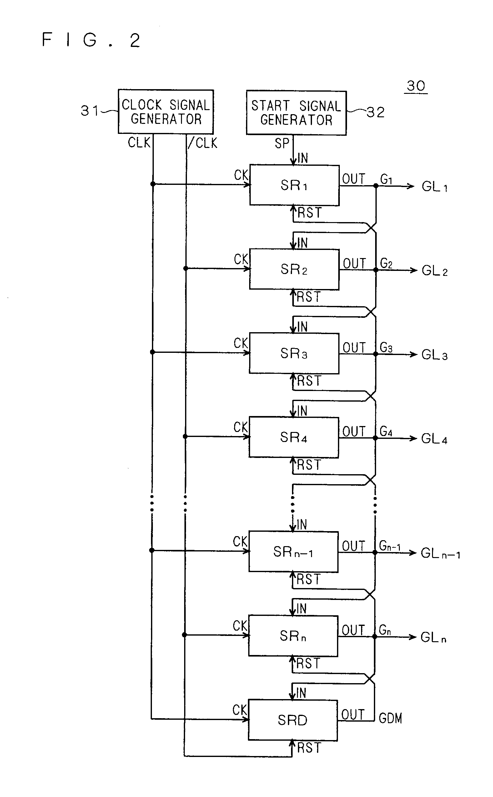
[0051]The liquid crystal display apparatus 100 includes a liquid crystal array unit 10, a gate line driving circuit (scanning line driving circuit) 30, and a source driver 40. As will be clear from the following description, a shift register according to the embodiments of the present invention is arranged in the gate line driving circuit 30.

[0052]The liquid crystal array unit 10 includes a plural...

second embodiment

[0186]FIG. 11 is a circuit diagram showing a configuration of a unit shift register according to the second embodiment. As shown in FIG. 11, in the present embodiment, a voltage generating circuit 33 for providing a predetermined potential VDD5 to the drain of the transistor Q9 is connected to the unit shift register SR according to the first embodiment (FIG. 3).

[0187]The voltage generating circuit 33 has a fifth power supply terminal S5 that is supplied with a high power supply potential VDD4, a voltage output terminal VT that outputs the potential VDD5, and at least one clock input terminal with which a predetermined clock signal is input (FIG. 11 shows a clock input terminal CKT as a representative example). In the present embodiment, one of the multi-phase clock signals that drive the plurality of cascade-connected unit shift register circuits SR (i.e., the gate line driving circuit 30) is used as the clock signal input to the clock input terminal (FIG. 11 shows a clock signal C...

third embodiment

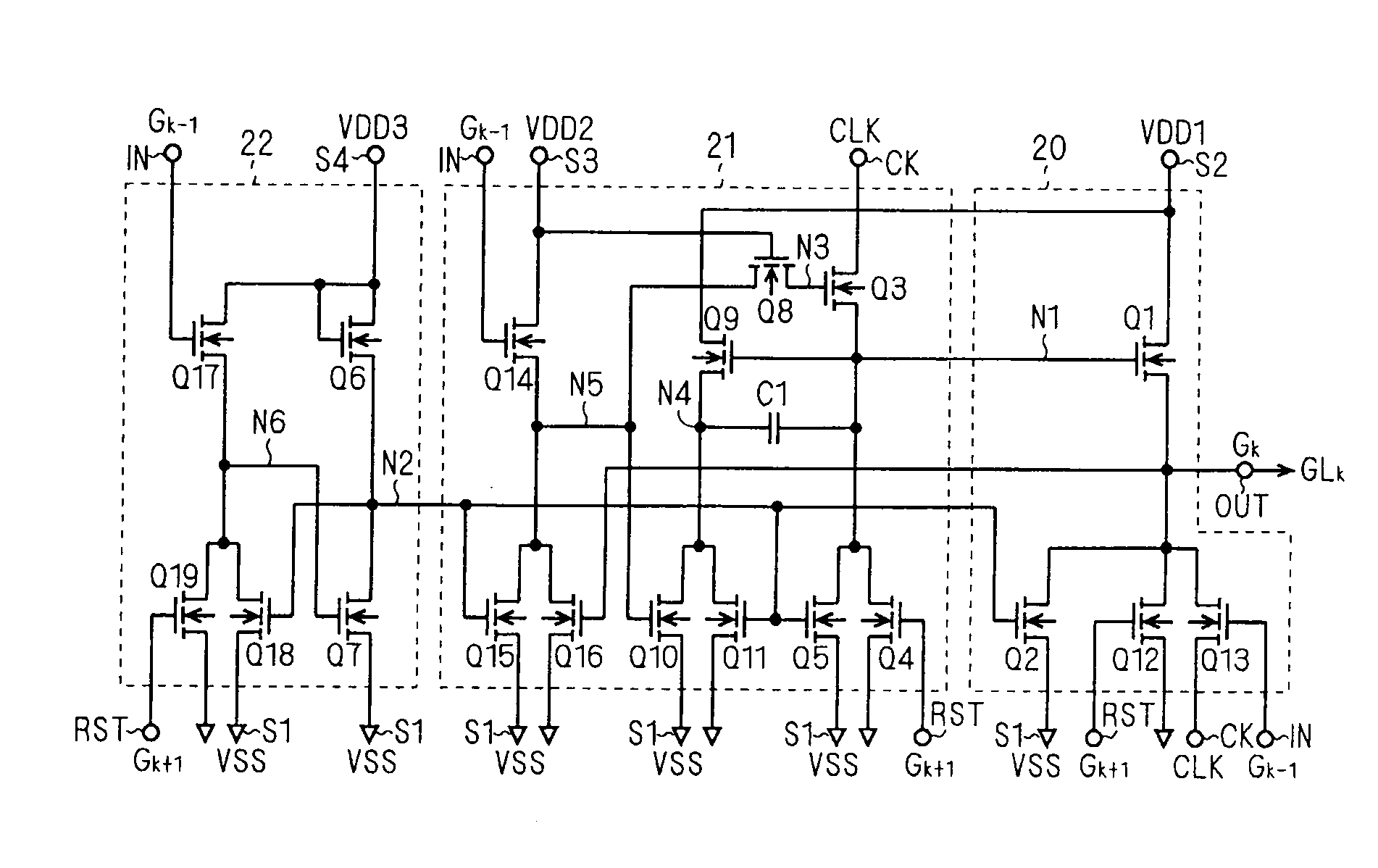
[0233]FIG. 16 is a circuit diagram showing the unit shift register SRk according to the third embodiment. Compared with the unit shift register SRk of FIG. 10, this unit shift register SRk is configured such that the drain of the transistor Q9 is connected to the voltage generating circuit 33 explained in the second embodiment.

[0234]In the unit shift register SRk of FIG. 16, the gate (node N1A) of the transistor Q9 is separated from the node N1 having a large parasitic capacitance. Compared with the capacitive element C1A, the parasitic capacitance of the node N1A is so small that it can almost be disregarded. Accordingly, when the level of the node N4 increases, the node N1A is increased to approximately VDD+VDD5. Therefore, the transistor Q9 operates in non-saturation region to rapidly charge the node N4 to the potential VDD5.

[0235]As a result, the potential at the node N1 is rapidly increased by the capacitive element C1, and the raised level of the node N1 is higher than that of...


PUM


Abstract

A shift register circuit is provided that can decrease a power consumption caused by a clock signal and can achieve a high driving capacity. A unit shift register has a first transistor that activates an output signal when a power supply potential is provided to an output terminal. A pull-up driving circuit for driving the first transistor has a second transistor for providing a clock signal to a node connected to the gate of the first transistor and a boosting circuit for the node. When an output signal of a preceding stage is activated, the second transistor turns on. Thereafter, when the clock signal is activated, and the node is charged, the second transistor turns off. The boosting circuit increases the potential at the node when the second transistor turns off. Therefore, the first transistor can operate in non-saturation region and activate the output signal.

Description

BACKGROUND OF THE INVENTION[0001]1. Field of the Invention[0002]The present invention relates to a scanning line driving circuit, and more particularly to a shift register circuit applicable to a scanning line driving circuit for use as, e.g., an electro-optic apparatus such as an image display apparatus and an image sensor and constituted by only field-effect transistors of the same conductivity type.[0003]2. Description of the Background Art[0004]In an image display apparatus (hereinafter referred to as a “display apparatus”) such as a liquid crystal display apparatus, a plurality of pixels are arranged in a matrix on a display panel, and a gate line (scanning line) is provided for each row of pixels (pixel line) of the display panel. In a cycle of one horizontal period of a display signal, the gate lines are sequentially selected and driven to update a display image. As a gate line driving circuit (scanning line driving circuit) for sequentially selecting and driving pixel lines,...

Claims


Application Information

Patent Timeline
Patent Type & Authority Applications(United States)
IPC IPC(8): G11C19/28G11C19/00
CPCG09G2310/0286G09G2330/021G11C19/184
Inventor TOBITA, YOUICHI
Owner TRIVALE TECH
Why Eureka
Try Eureka