Circuits for biasing/charging high impedance loads

a high impedance load and circuit technology, applied in the field of circuit arrangement, can solve the problems of inability to passively filter, undesirable rapid rise in noise with leakage above such a knee, inability to bias voltage generator inherently noisy, etc., and achieve the effect of more rapid charging, low voltage on the output terminal, and rapid charging of the devi

Inactive Publication Date: 2010-07-01
WOLFSON MICROELECTRONICS LTD
View PDF12 Cites 12 Cited by
  • Summary
  • Abstract
  • Description
  • Claims
  • Application Information

AI Technical Summary

Benefits of technology

[0034]The shunt device is configured to pass current when the voltage level on the output terminal is below a threshold level and to pass substantially no current when the voltage level on the output terminal is above a threshold level. In other words, at device start up, the voltage on the output terminal may be low. In this case the shunt device allows current to pass to allow rapid charging of the device. However once the voltage level reaches the threshold level the shunt device ceases to pass current leaving the reverse bias diode as the charging path. The reverse current through the reverse bias diode can then complete any necessary charging to bring the output terminal up to the final operating voltage / current level and can allow sufficient current to pass to compensate for any leakage current. The threshold voltage may be a fixed threshold, i.e. a certain defined voltage, or may be a relative threshold, i.e. a certain voltage difference. The threshold level may be substantially the operating voltage of the capacitive load. The threshold level may be, for instance, within about 1V of the operating voltage of the capacitive load.
[0035]To allow for more rapid charging than possible through the reverse bias diode alone, the shunt device is configured to pass a current which is larger than the reverse current of the reverse bias diode when the voltage level on the output terminal is lower than the threshold level.

Problems solved by technology

For microphones, for example, the wide dynamic range of audio signals, from deafening overload to almost inaudible, results in an output voltage level of a few millivolts for normal sound levels and a requirement for equivalent total input noise level within the audio band of only a few microvolts.
Such an amplified bias voltage generator will be inherently noisy, yet any audio band noise on its output will cause a signal at the other end of the transducer that is indistinguishable from a similar audio noise stimulus.
However, even these low currents may cause the diode to conduct strongly enough to couple audio band noise onto the bias node.
The small size of the microphone package, and stringent cost constraints preclude a reservoir capacitor of more than a few tens of picofarads since a larger on-chip capacitor would take up excessive chip area and a discrete capacitor would not fit in the small package, so a passive filter is not practical due to the excessive resistor size (of the order of gigaohms) that would be required.
Such a rapid rise in noise with leakage above such a knee is undesirable.

Method used


Image

  • Circuits for biasing/charging high impedance loads
  • Circuits for biasing/charging high impedance loads
  • Circuits for biasing/charging high impedance loads

Examples


Embodiment Construction

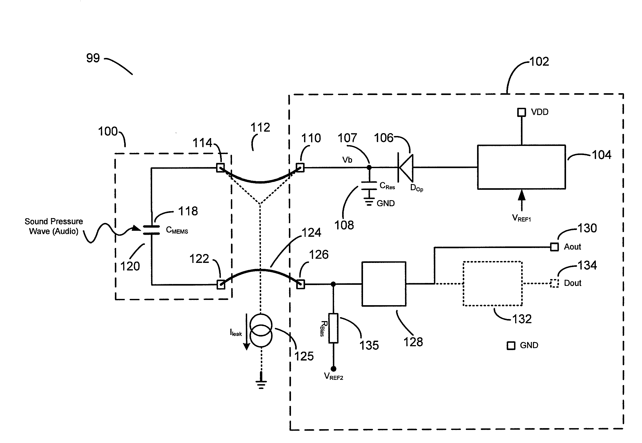
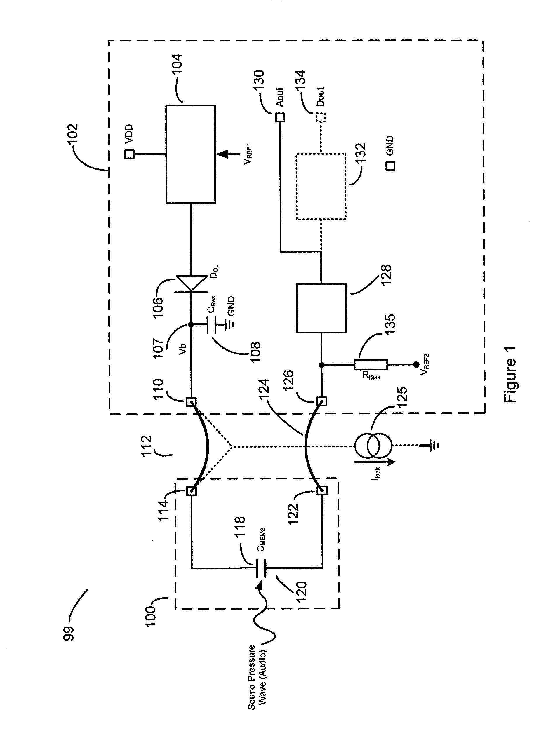
[0065]The embodiments below will be described in relation to charging a capacitive transducer such as a MEMS microphone. However it is noted that the invention is suitable not only for charging or biasing any type of capacitive load but also with other applications where charging or biasing is required with low noise. The skilled person will appreciate that a capacitive load can be regarded as a high impedance load and the invention is suitable for biasing other high impedance loads.

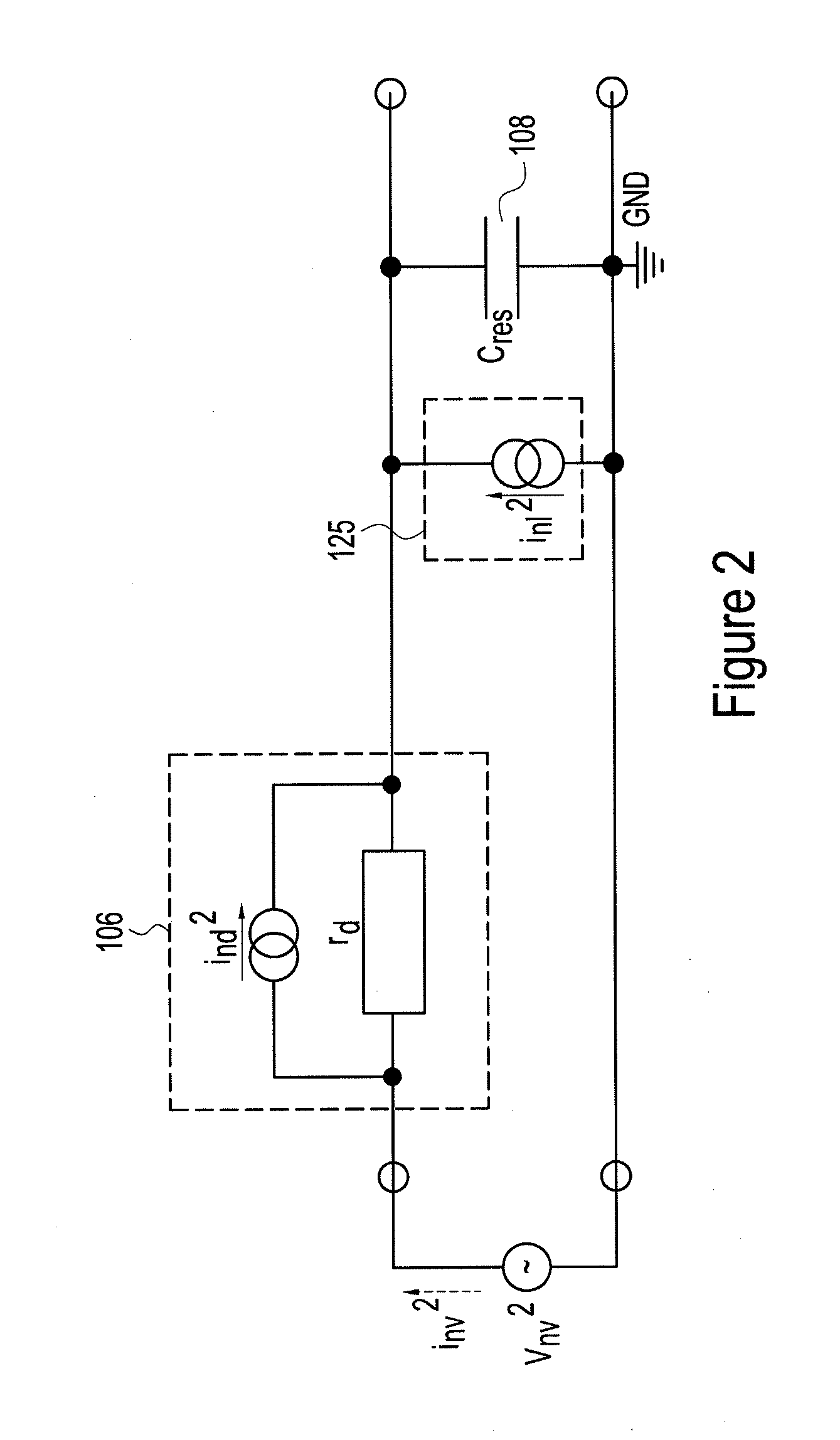
[0066]In an embodiment of the present invention, the forward biased diode 106 in FIG. 1 is replaced by a reverse biased diode DR 206 as shown in FIG. 4.

[0067]The reverse biased diode is preferably what may be referred to as a leaky diode i.e. it allows some current to flow from node X to node Y when reverse biased, i.e. it allows a small reverse current. Such leaky current flow is advantageous as it allows the voltage bias means to supply a current to compensate for any leakage current associated with th...


PUM


Abstract

A charging circuit for charging/biasing high impedance loads such as capacitive loads. The circuit comprises an input for connecting to a voltage/charge source and an output for connecting to the load. A capacitor is connected between the output and a reference voltage such as ground and a reverse bias diode is connected between the input and the output terminals. The reverse bias diode is arranged to allow a reverse current to pass which is sufficient to compensate for current leakage at the output terminal or other parts of the circuit. The reverse bias diode is conveniently a polysilicon diode. The diode may be connected in parallel with a shunt device to allow for rapid charging during start up.

Description

BACKGROUND OF THE INVENTION[0001]1. Field of the Invention[0002]The present invention relates to a circuit arrangement for use in biasing or charging circuits, especially for biasing or charging of capacitive loads and in particular MEMS transducers.[0003]2. Description of the Related Art[0004]Consumer electronics devices are continually getting smaller and, with advances in technology, are gaining ever increasing performance and functionality. This is clearly evident in the technology used in consumer electronic products such as mobile phones, laptop computers, MP3 players and personal digital assistants (PDAs). Requirements of the mobile phone industry for example, are driving the components to become smaller with higher functionality and reduced cost. For example, some mobile phones now require multiple microphones for noise cancelling, or accelerometers to allow inertial navigation, while maintaining or reducing the small form factor and aiming at a similar total cost to previou...

Claims


Application Information

Patent Timeline
Patent Type & Authority Applications(United States)
IPC IPC(8): H04R3/00H02J7/00
CPCH04R19/005H04R19/016H04B1/1018H04B1/1607H04B15/005
Inventor PENNOCK, JOHN LAURENCE
Owner WOLFSON MICROELECTRONICS LTD
Why Eureka
Try Eureka