Method for manufacturing touch panel, touch panel, display device, and electronic apparatus

a technology of display device and touch panel, which is applied in the direction of liquid/solution decomposition chemical coating, superimposed coating process, instruments, etc., can solve the problems of increasing manufacturing cost, reduce manufacturing cost, reduce manufacturing cost, the effect of reducing the number of steps for forming the first and second electrodes

Inactive Publication Date: 2010-07-08
SEIKO EPSON CORP
View PDF12 Cites 121 Cited by
  • Summary
  • Abstract
  • Description
  • Claims
  • Application Information

AI Technical Summary

Benefits of technology

[0010]An advantage of the invention is to provide a method for manufacturing a touch panel, a touch panel, a display device, and an electronic apparatus that are capable of reducing manufacturing costs.
[0011]According to a first aspect of the invention, a method for manufacturing a touch panel including a substrate, a first electrode, and a second electrode, the first and second electrodes being formed on one side of the substrate in a plural numbers and extending in directions intersecting with each other, the method includes forming the first electrode and electrode films on the substrate, forming an insulating film by a printing method on at least an intersection of the first electrode with the second electrode, and forming a bridge wiring line connecting the electrode films over the insulating film by the printing method. In the method, each of the electrode films has a shape obtained by cutting off the second electrode at the intersection.
[0012]According to the first aspect, the first electrode and the electrode films to serve as the second electrode are formed in the same step, and the bridge wiring line connecting the electrode films is formed by the printing method. In this way, the number of steps for forming the first and second electrodes can be reduced. As a result, it is possible to provide a method for manufacturing a touch panel capable of reducing manufacturing costs.
[0013]In the method for manufacturing a touch panel, the first and second electrodes may respectively have a plurality of island-shaped electrode portions and a bridge wiring line connecting the island-shaped electrode portions adjacent to each other while the bridge wiring line of the first electrode intersects with the bridge wiring line of the second electrode. In forming the first electrode and the electrode films, the first electrode and the island-shaped electrode portions of ...

Problems solved by technology

However, in the first to fourth examples above, when the electrodes extending in respective directions are formed or when the electrode and an active circuit are formed on the sa...

Method used


Image

  • Method for manufacturing touch panel, touch panel, display device, and electronic apparatus
  • Method for manufacturing touch panel, touch panel, display device, and electronic apparatus
  • Method for manufacturing touch panel, touch panel, display device, and electronic apparatus

Examples


first embodiment

Touch Panel

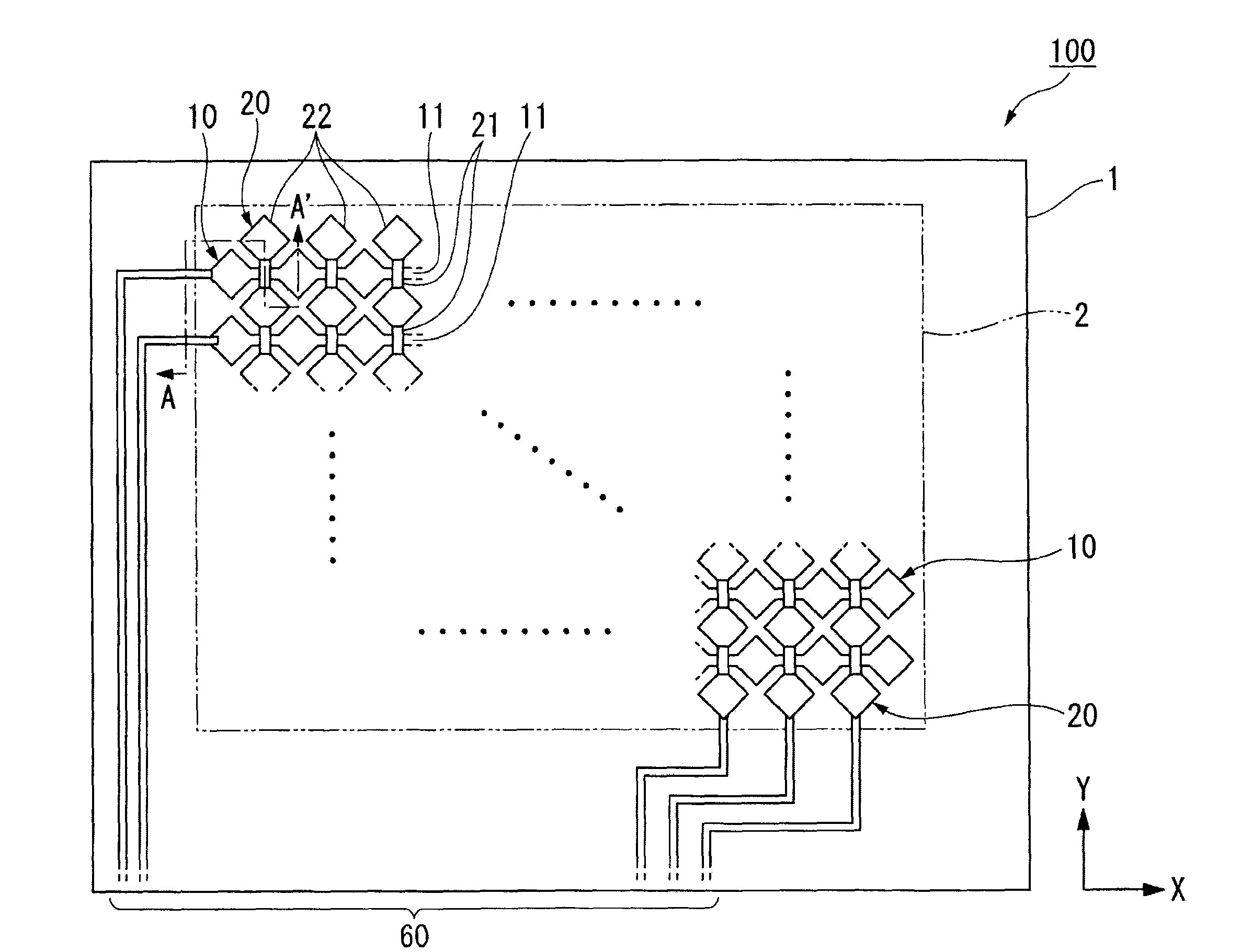
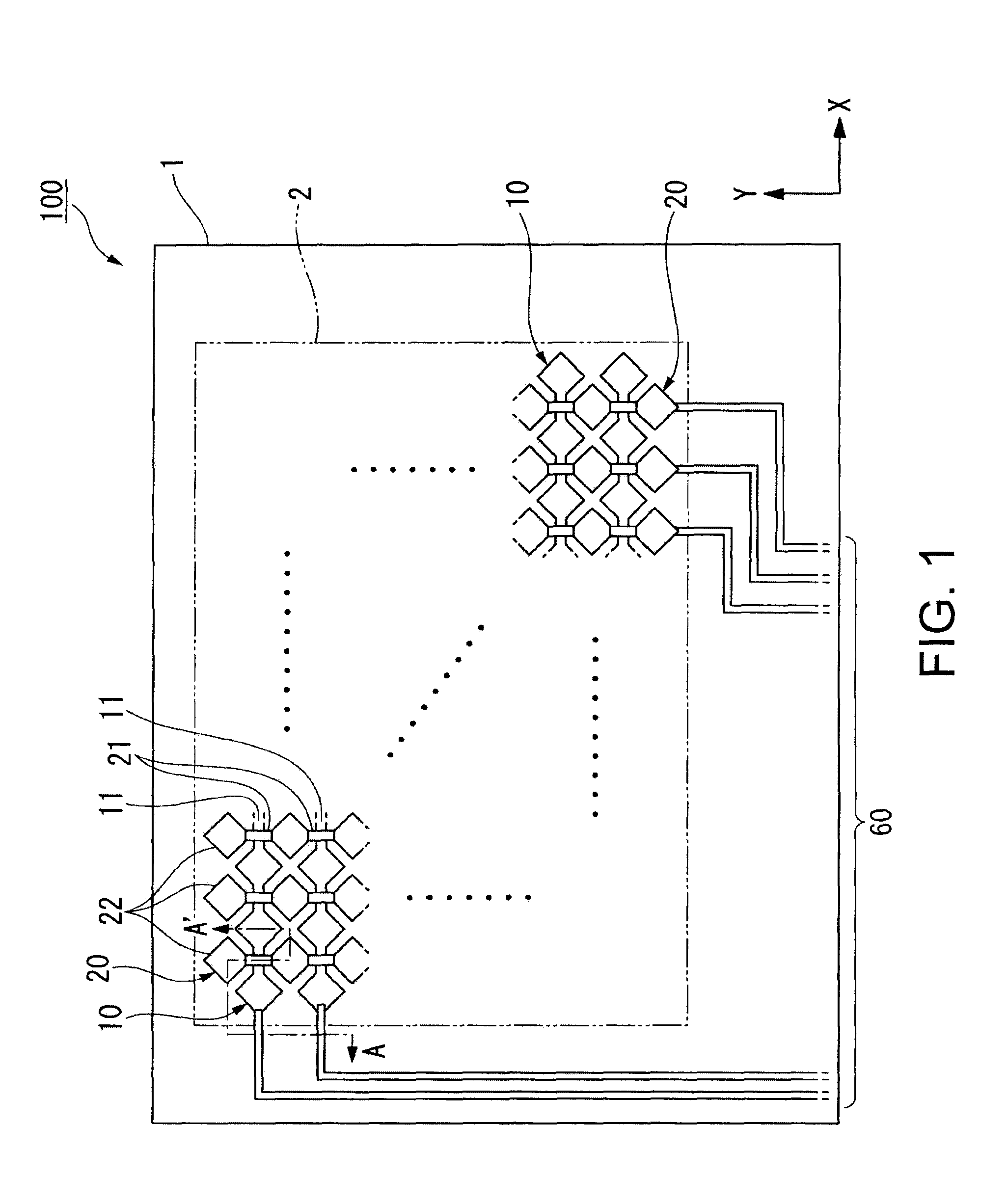
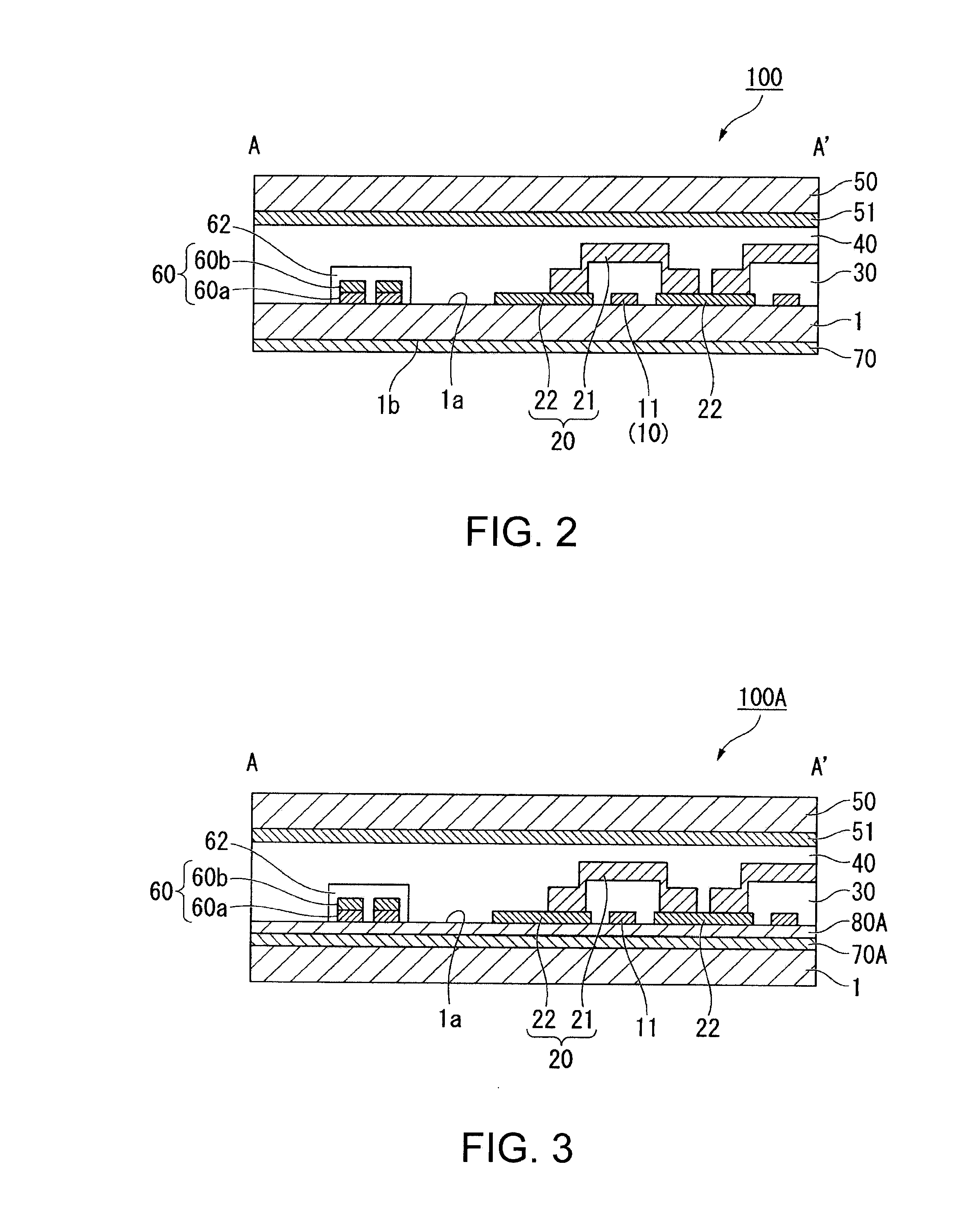
[0053]FIG. 1 is a schematic plan view showing a touch panel 100 according a first embodiment of the invention. FIG. 2 is a sectional view taken along the line A-A′ of the touch panel 100.

[0054]The touch panel 100 includes a substrate 1, an input area 2, and interconnection wiring lines 60. The substrate 1 is formed in a rectangular shape in a plan view, and is made of a transparent material such as glass or acrylic resin.

[0055]The input area 2 is an area enclosed by dashed lines in FIG. 1, and detects positional information on a finger that brought close to the touch panel. In the input area 2, a plurality of X-electrodes 10 and a plurality of Y-electrodes 20 are respectively arranged. In the drawing, each of the X-electrodes 10 extends in an X-axis direction and the plurality of X-electrodes 10 is arranged along a Y-axis direction, whereas each of the Y-electrodes 20 extends in the Y-axis direction and the plurality of Y-electrodes 20 is arranged along the X-axis directi...

second embodiment

[0116]A touch panel according to a second embodiment of the invention will be described. FIG. 11 is a schematic sectional view showing a touch panel 200 according to the second embodiment of the invention. FIG. 12 is a schematic sectional view taken along the line B-B′ of the touch panel 200. In the present embodiment, detailed descriptions of portions having the same structure as those of the touch panels 100 and 100A shown in FIGS. 1 through 3 may be adequately omitted.

[0117]As shown in FIG. 11, the touch panel 200 includes the substrate 1, the input area 2, and the interconnection wiring lines 60.

[0118]The substrate 1 is formed in a rectangular shape in a plan view, and is made of a transparent material such as glass or acrylic resin.

[0119]The input area 2 is an area enclosed by dashed lines in FIG. 11, and detects positional information on a finger that brought close to the touch panel. In the input area 2, a plurality of X-electrodes 110 and a plurality of Y-electrodes 120 are ...


PUM

PropertyMeasurementUnit
Shapeaaaaaaaaaa
Electrical conductoraaaaaaaaaa
Areaaaaaaaaaaa

Abstract

A method for manufacturing a touch panel including a substrate, a first electrode, and a second electrode, the first and second electrodes being formed on one side of the substrate in a plural numbers and extending in directions intersecting with each other, the method includes forming the first electrode and electrode films on the substrate, forming an insulating film by a printing method on at least an intersection of the first electrode with the second electrode, and forming a bridge wiring line connecting the electrode films over the insulating film by the printing method. In the method, each of the electrode films has a shape obtained by cutting off the second electrode at the intersection.

Description

BACKGROUND[0001]1. Technical Field[0002]The present invention relates to a method for manufacturing a touch panel, a touch panel, a display device, and an electronic apparatus.[0003]2. Related Art[0004]In capacitance touch screens, when a finger is brought close to a predetermined position of a panel in which electrodes are formed, capacitance is formed between the electrodes. The predetermined position is detected by detecting a current for charging the capacitance. As the capacitance touch screens, the followings are disclosed, for example.[0005]JP-A-4-337824 is a first example of related art. In a coordinate input device disclosed in the first example, a substrate including X-electrodes and a substrate including Y-electrodes support a liquid crystal layer. Then, an electrode of a detection pen brought close to the substrate including the X-electrodes forms stray capacitance between the X- and Y-electrodes. A position of the detection pen is detected by a voltage induced when the ...

Claims


Application Information

Patent Timeline
IPC IPC(8): G06F3/041B05D5/12
CPCG06F3/044G06F2203/04111G06F3/0445G06F3/0446
Inventor DENDA, ATSUSHI
Owner SEIKO EPSON CORP
Why Eureka
Try Eureka