Switching power supply device and switching power supply control circuit

Active Publication Date: 2010-07-08
FUJI ELECTRIC CO LTD
View PDF10 Cites 36 Cited by
  • Summary
  • Abstract
  • Description
  • Claims
  • Application Information

AI Technical Summary

Benefits of technology

[0038]By means of this invention, a light loading state is expressed by the time difference between the conduction timing of a diode rectifying element or of the internal diode of a synchronous rectification switching element, and the turn-on timing of a main switching element, so that by comparing this time difference with a reference time signal, a light loading state can be detected by a logic circuit alone, and at the same time the light loading state can be detected without affecting power efficiency.
[0039]Further, when a plurality of synchronous rectification switching elements, with internal diodes connected in parallel, are provided on the secondary side of the transformer, the gate on/off signals applied to the gates of the main switching elements and a maximum on-width signal are utilized to enable control of the on intervals of synchronous rectification switching elements, so that all noise can be eliminated outside the times at which the main

Problems solved by technology

However, when using such a switching power supply device as a low-voltage, large-current power supply, when secondary currents I1 and I2 flow in the rectifying diodes D1 and D2 provided on the secondary side of the transformer T, large current losses VF×IO due to the forward-direction voltage drop VF across the rectifying diodes D1, D2 occur.
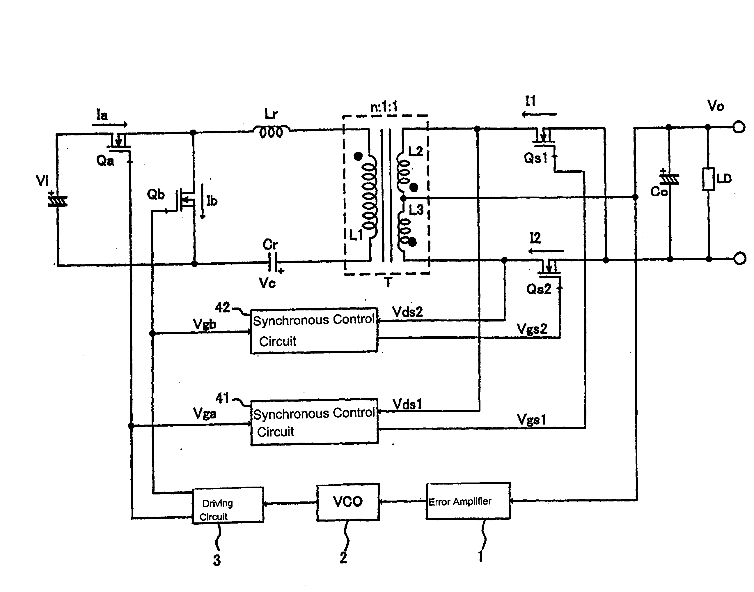
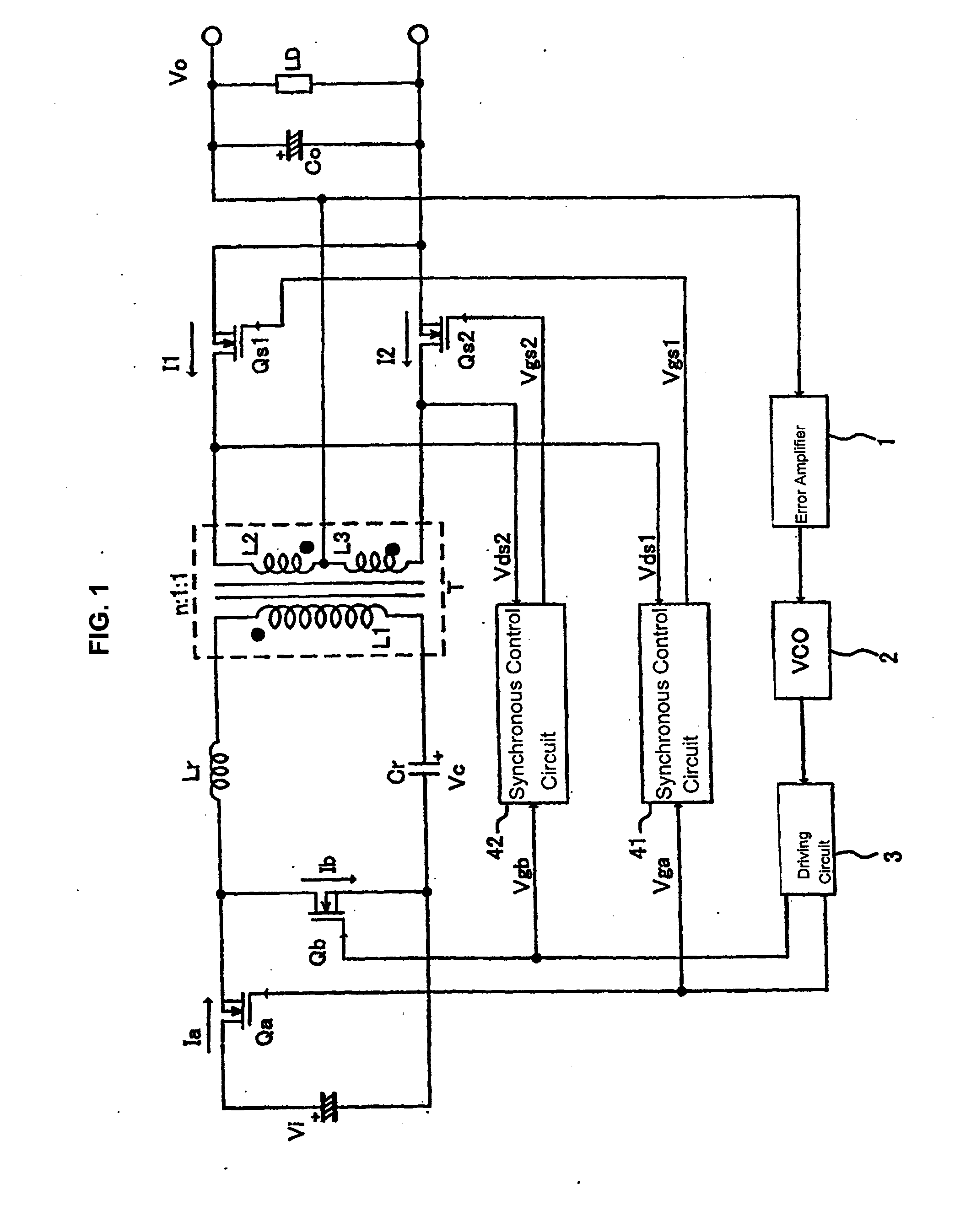
Such a switching power supply device of the prior art is configured so as to cause the main switching elements Qa, Qb to perform switching operation, to obtain an arbitrary DC output via the voltage-conversion transformer T. In such a device, charge accumulated on the capacitor CO is discharged, according to the magnitude and similar of the load LD connected to the secondary side, so that current flowing back to the transformer T (back current) occurs, and the problem of power loss in the backflow region arises.
Further, there is the concern of circuit destruction due to the backflow of power to the primary side of the transformer T.
Hence while synchronous rectification in which the synchronous driving signals Vgs1, Vgs2 are completely synchronized with the power switching signals as shown in FIG. 8 is a simple method, in this case the five backflow regions described below pose problems, and measures to resolve these problems are necessary.
This is because in the very light loading (VLL) state, little energy is sent to the secondary side, and so resonance operation ends in a short length of time.
In this way, in the invention described in U.S. Patent Application No. 2008/0055942, high-frequency oscillation is repeated each time the secondary current Is decreases to reach zero, and so this method poses problems from the standpoints of noise and power conversion efficiency.
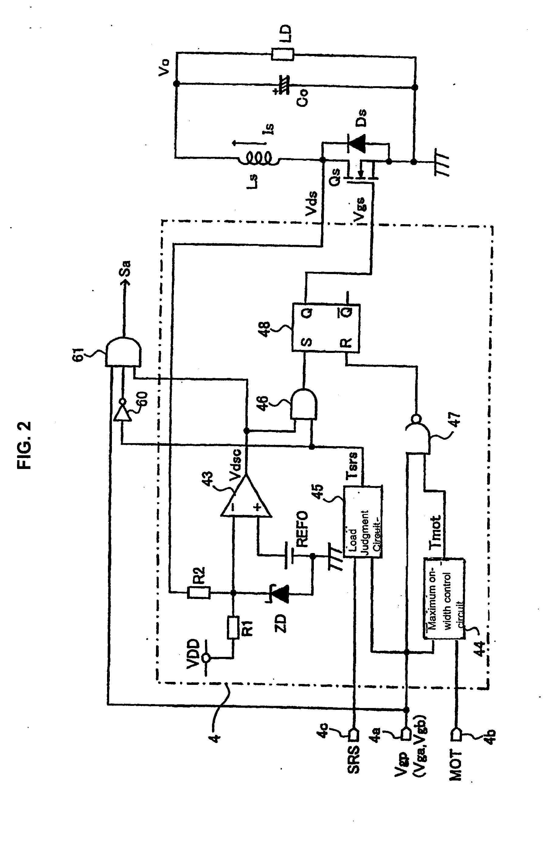
Here, the turn-on timing of the synchronous driving signal is

Method used


Image

  • Switching power supply device and switching power supply control circuit
  • Switching power supply device and switching power supply control circuit
  • Switching power supply device and switching power supply control circuit

Examples


Embodiment Construction

[0060]FIG. 1 is a circuit diagram showing the overall configuration of the switching power supply device of an aspect. The switching power supply device is configured such that an input DC voltage Vi is applied to a series resonance circuit having a resonance inductor Lr and a resonance capacitor Cr, and a prescribed output voltage VO for a load LD is generated via a transformer T. MOSFETs Qa, Qb are main switching elements which switch the current path to the series resonance circuit by switching in alternation on the primary side of the transformer T. One end of the resonance inductor Lr is connected to one end of the primary windings L1 of the transformer T, and the other end of the primary windings L1 is connected to one end of the resonance capacitor Cr. A configuration may be employed in which no inductance other than that of the transformer T is provided, and the linkage inductance of the transformer T is employed as a current resonance inductor. Also, a configuration may be ...


PUM


Abstract

The invention provides a switching power supply device which can detect a light load state on a pulse-by-pulse basis without worsening power efficiency. In a synchronous control circuit, for each timing of the turning-on of main switching elements, the delay time Tdif of the conduction timing of internal diodes Ds determined according to the magnitude of the load LD is detected by a comparator, a reference time pulse Tsrs having a prescribed time width is generated by a load judgment circuit, and the logical product of the two is generated by an AND circuit. By this means, the load is regarded as being a light load when the delay time Tdif is longer than the reference time pulse Tsrs, and the synchronous rectification MOSFETs Qs are not turned on.

Description

BACKGROUND OF THE INVENTION[0001]The invention relates to a switching power supply device and switching power supply control circuit comprising a series resonance circuit having a current resonance inductor and a current resonance capacitor, and in particular relates to a switching power supply device and switching power supply control circuit which eliminated backflow of current under light loading.[0002]Switching power supply devices comprising current resonance-type converters such as that shown in FIG. 7 are known as switching power supply devices of the prior art. In such current resonance converters, an input DC voltage Vi is applied to a series resonance circuit having a resonance inductor Lr and a resonance capacitor Cr, and two main switching elements Qa, Qb, comprising MOSFETs (Metal-Oxide-Semiconductor Field-Effect Transistors) or similar, are turned on and off to control the path of the primary-side current flowing in the primary windings L1 of a power conversion transfo...

Claims


Application Information

Patent Timeline
IPC IPC(8): H02M3/335
CPCH02M3/33592H02M3/337H02M2001/0032Y02B70/1491Y02B70/16H02M2001/0058Y02B70/1475Y02B70/10H02M1/0032H02M1/0058H02M3/33573H02M3/33571H02M3/01
Inventor CHEN, JIANSONOBE, KOJI
Owner FUJI ELECTRIC CO LTD
Why Eureka
Try Eureka