Organic light emitting display device and method of manufacturing the same

a light-emitting display and organic technology, applied in the direction of organic semiconductor devices, thermoelectric devices, electroluminescent light sources, etc., can solve the problems of insufficient use of amorphous igzo, uneven threshold voltage, difficult implementation of amorphous silicon in driving circuits operating at high speeds, etc., to achieve stable and uniform functional properties, high carrier concentration, and high charge mobility

Active Publication Date: 2010-07-15
SAMSUNG DISPLAY CO LTD
View PDF6 Cites 95 Cited by
  • Summary
  • Abstract
  • Description
  • Claims
  • Application Information

AI Technical Summary

Benefits of technology

[0016]The organic light emitting display device according to the present invention includes the thin film transistor of the drive unit that has the activation layer formed in a structure where the first oxide semiconductor layer and the second oxide semiconductor layer are stacked, the thin film transistor of the pixel unit that has the activation layer formed of the second oxide semiconductor layer, and the organic light emitting diode physically coupled to the thin film transistor of the pixel unit. The thin film transistor of the drive unit has a channel formed on the first oxide semiconductor layer having a higher carrier concentration than the second oxide semiconductor layer, having a high charge mobility. The thin film transistor of the pixel unit has a channel formed on the second oxide semiconductor layer, so that the thin film transistor of the pixel unit has a stable and uniform functional property.

Problems solved by technology

In general, the amorphous silicon has a low mobility, therefore, the amorphous silicon is difficult to be implemented in a driving circuit which operates at a high speed.
However, the poly-silicon has a disadvantage that threshold voltage is uneven due to the nature of polycrystalline, and the low temperature poly-silicon has a disadvantage that a laser annealing or other related process for crystallization may be required during the manufacture of the poly-silicon.
The amorphous IGZO is however insufficient for being used as the activation layer of the thin film transistor of the drive unit where a high charge mobility (about 100 cm2 / V·sec) at a level of the low temperature poly-silicon is required.
Therefore, significant problems may occur in stable property distribution and reliability of the thin film transistor of the drive unit.

Method used


Image

  • Organic light emitting display device and method of manufacturing the same
  • Organic light emitting display device and method of manufacturing the same
  • Organic light emitting display device and method of manufacturing the same

Examples


Embodiment Construction

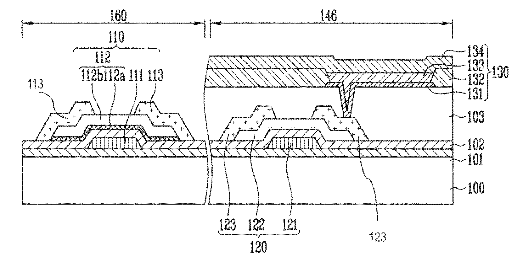
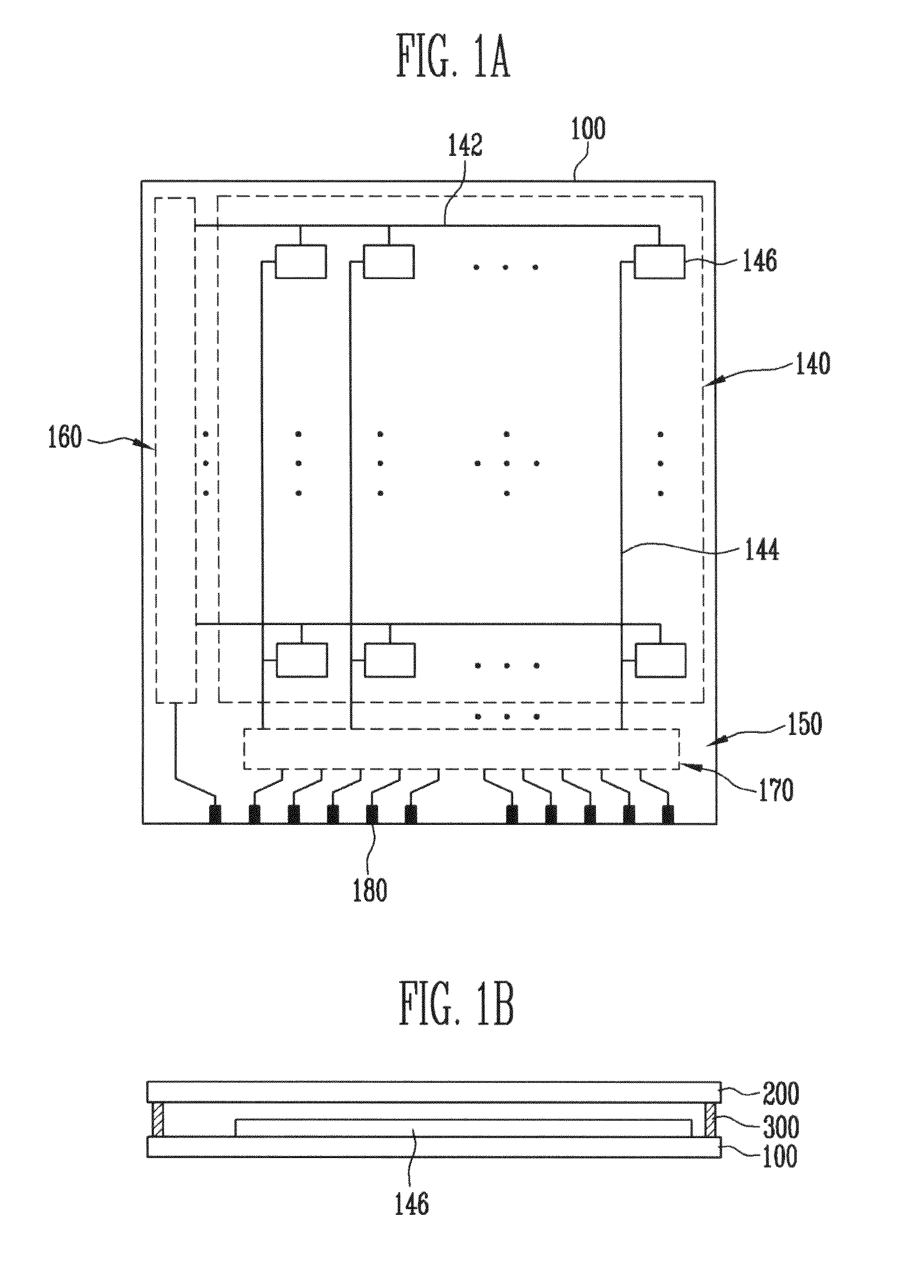
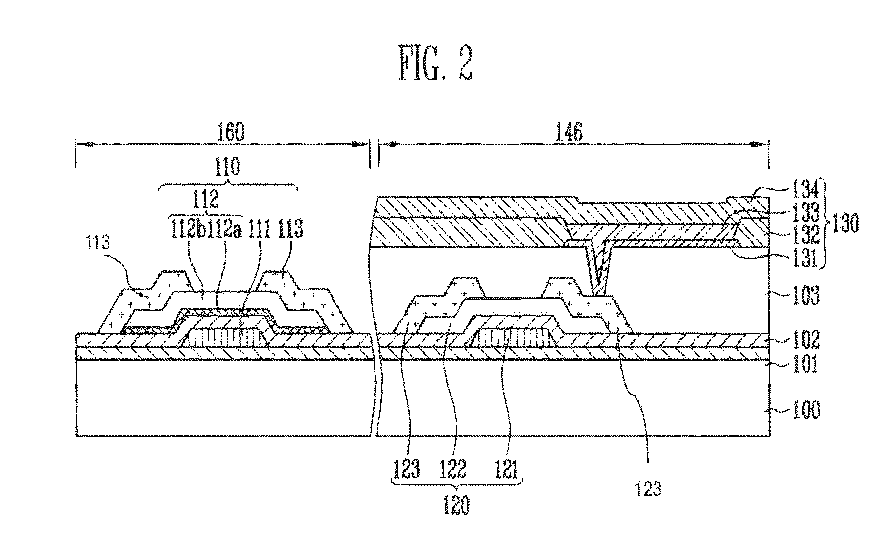
[0023]In the following detailed description, only certain exemplary embodiments of the present invention have been shown and described, simply by way of illustration. As those skilled in the art would realize, the described embodiments may be modified in various different ways, all without departing from the spirit or scope of the present invention. Accordingly, the drawings and description are to be regarded as illustrative in nature and not restrictive. Accordingly, the drawings and description are to be regarded as illustrative in nature and not restrictive.

[0024]In addition, when an element is referred to as being “on” another element, it can be directly on the another element or be indirectly on the another element with one or more intervening elements interposed therebetween. Also, when an element is referred to as being “connected to” another element, it can be directly connected to the another element or be indirectly connected to the another element with one or more interve...


PUM


Abstract

Disclosed is an organic light emitting display device and a method of manufacturing the same. The organic light emitting display device includes the thin film transistor of the drive unit that has the activation layer formed in a structure where the first oxide semiconductor layer and the second oxide semiconductor layer are stacked, the thin film transistor of the pixel unit that has the activation layer formed of the second oxide semiconductor layer, and the organic light emitting diode coupled to the thin film transistor of the pixel unit. The thin film transistor of the drive unit has channel formed on the first oxide semiconductor layer having a higher carrier concentration than the second oxide semiconductor layer, having a high charge mobility, and the thin film transistor of the pixel unit has a channel formed on the second oxide semiconductor layer, having a stable and uniform functional property.

Description

CLAIM OF PRIORITY[0001]This application makes reference to, incorporates the same herein, and claims all benefits accruing under 35 U.S.C. §119 from an application earlier filed in the Korean Intellectual Property Office on 12 Jan. 2009 and there duly assigned Serial No. 10-2009-0002242.BACKGROUND OF THE INVENTION[0002]1. Field of the Invention[0003]The present invention relates to an organic light emitting display device and a method of manufacturing the same, and more particularly, to an organic light emitting display device that has a difference in charge mobility between a thin film transistor of a drive unit and a thin film transistor of a pixel unit, and a method of manufacturing the same.[0004]2. Discussion of Related Art[0005]An organic light emitting display device is a next generation display device which may actively emit light. Compared to a liquid crystal display device (LCD), the organic light emitting display device has excellent characteristics in view of view angle,...

Claims


Application Information

Patent Timeline
Patent Type & Authority Applications(United States)
IPC IPC(8): H01L51/52H01L51/56H01L33/00H05B44/00
CPCH01L2251/305H01L27/3262H01L27/1225H01L27/1229H10K59/1213H10K2102/101
Inventor PARK, JIN-SEONGMO, YEON-GONJEONG, JAE-KYEONGKIM, MIN-KYUCHUNG, HYUN-JOONGAHN, TAE-KYUNG
Owner SAMSUNG DISPLAY CO LTD
Why Eureka
Try Eureka