Thin film transistor, method of manufacturing the same and flat panel display device having the same

a technology of thin film transistors and flat panels, which is applied in the direction of transistors, solid-state devices, thermoelectric devices, etc., can solve the problems of plasma damage, difficult control of the properties of the resultant transistors, and difficulty in implementing a high-speed driving circuit, so as to prevent the deterioration of electrical properties and the degree of dispersion of electrical properties

Inactive Publication Date: 2010-07-15
SAMSUNG DISPLAY CO LTD
View PDF29 Cites 32 Cited by
  • Summary
  • Abstract
  • Description
  • Claims
  • Application Information

AI Technical Summary

Benefits of technology

[0011]Aspects of the present invention provide a thin film transistor which can prevent the deterioration of electrical properties and the degree of dispersion thereof due to damage of an activation layer, a method of manufacturing the thin film transistor, and a flat panel display device having the thin film transistor. Aspects of the present invention provide a thin film transistor which can be applied to a large substrate in order to make a large display device, a method of manufacturing the thin film transistor, and a flat panel display device having the thin film transistor.

Problems solved by technology

However, if the activation layer is formed of the amorphous silicon, it is difficult to implement a high speed driving circuit due to low electron / hole mobility therein; and if the activation layer is formed of the poly-silicon, a separate compensation circuit should be added due to an uneven threshold voltage, despite high electron / hole mobility.
Also, a conventional method of manufacturing the thin film transistor using a low temperature poly-silicon (LTPS) includes an expensive process, such as a laser annealing, etc., and is difficult to control the properties of the resultant transistors.
However, if the compound semiconductor is used, when forming a thin film on an upper portion of the activation layer or etching the formed thin film, damage due to plasma is generated such that a change in an electrical property is generated.
Because of the deterioration of the electrical properties of the compound semiconductor, a change in threshold voltage of the thin film transistor, etc., and a degree of dispersion of the electrical properties within a substrate deteriorate.
However, in a thin film transistor having an activation layer formed of a compound semiconductor including oxygen, if a passivation layer is formed of silicon oxide SiO2, silicon nitride SiNx or aluminum oxide Al2O3, it causes deterioration in electrical properties.
If the damage due to plasma is generated, carrier concentration of the activation layer may be increased because of oxygen deficiency, off current may be increased because of such an excess carrier, and an S-factor property may deteriorate.

Method used


Image

  • Thin film transistor, method of manufacturing the same and flat panel display device having the same
  • Thin film transistor, method of manufacturing the same and flat panel display device having the same
  • Thin film transistor, method of manufacturing the same and flat panel display device having the same

Examples


Embodiment Construction

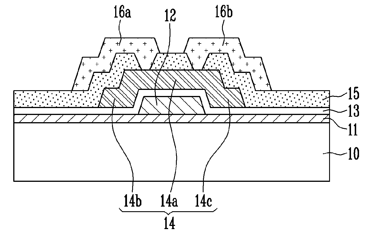
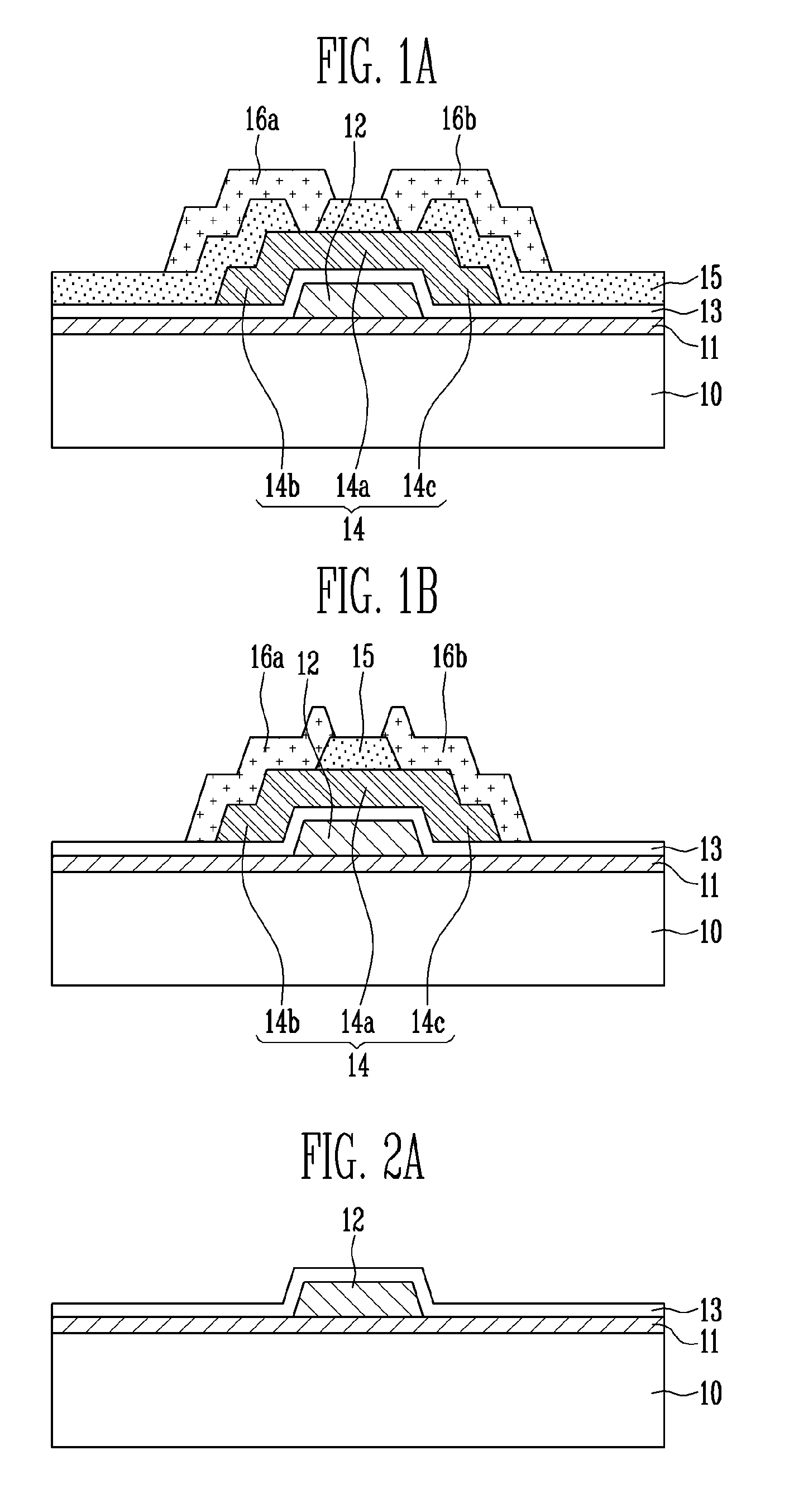
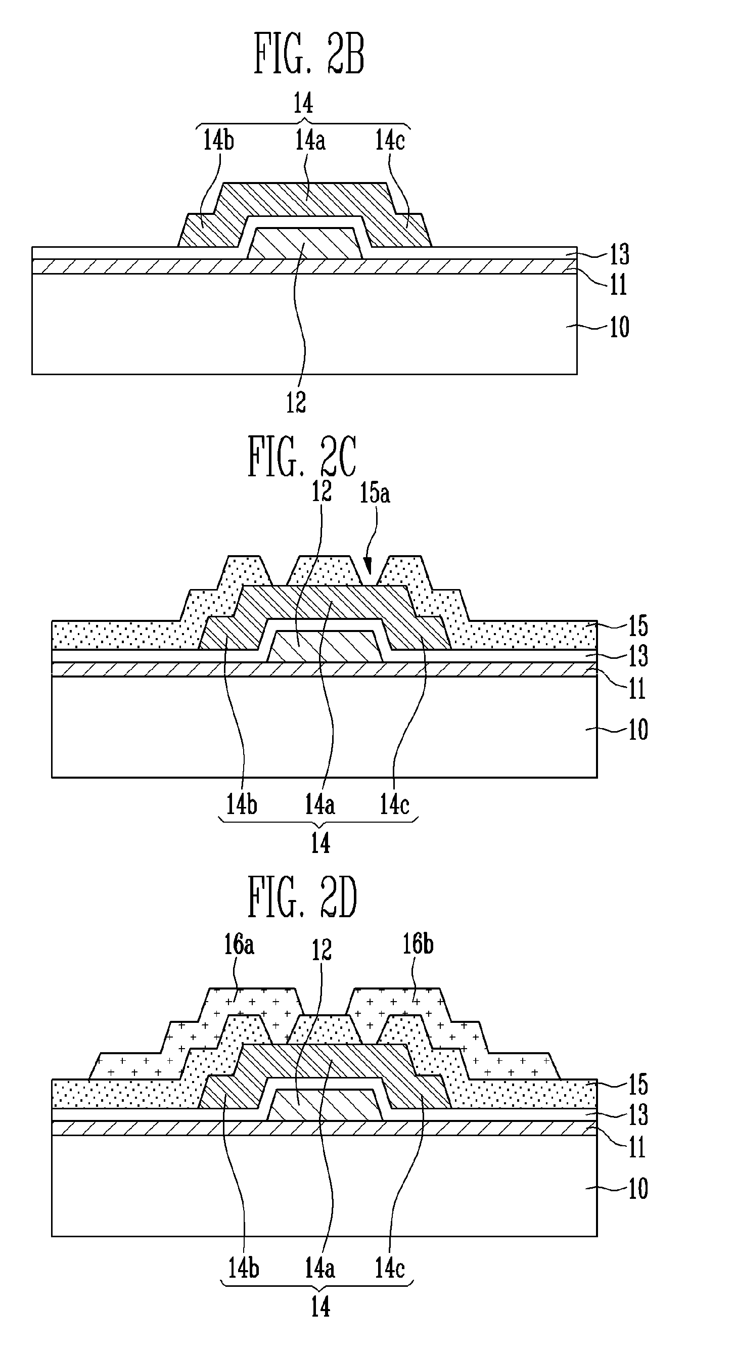
[0025]Reference will now be made in detail to the present embodiments of the present invention, examples of which are illustrated in the accompanying drawings, wherein like reference numerals refer to the like elements throughout. The embodiments are described below in order to explain the present invention by referring to the figures.

[0026]In the following detailed description, only certain exemplary embodiments of the present invention have been shown and described, simply by way of illustration. As those skilled in the art would realize, the described embodiments may be modified in various different ways, all without departing from the spirit or scope of the present invention. Accordingly, the drawings and description are to be regarded as illustrative in nature and not restrictive. In addition, when an element is referred to as being “on,”“formed on,” or “disposed on” another element, it can be directly on another element or be indirectly on the element with one or more interven...


PUM


Abstract

A thin film transistor which has a compound semiconductor including oxygen as an activation layer, a method of manufacturing the thin film transistor, and a flat panel display device having the thin film transistor, of which the thin film transistor comprises: a gate electrode formed on a substrate; an activation layer formed on the gate electrode, insulated from the gate electrode by a gate insulating film, and formed of a compound semiconductor including oxygen; a passivation layer formed on the activation layer; and source and drain electrodes formed to contact the activation layer, wherein the passivation layer includes titanium oxide (TiOx) or titanium oxynitride (TiOxNy).

Description

CROSS-REFERENCE TO RELATED APPLICATIONS[0001]This application claims the benefit of Korean Patent Application No. 10-2009-0002240, filed on Jan. 12, 2009, in the Korean Intellectual Property Office, the content of which is incorporated herein by reference.BACKGROUND OF THE INVENTION[0002]1. Field of the Invention[0003]Aspects of the present invention relate to a thin film transistor, a method of manufacturing the same, and a flat panel display device having the same.[0004]2. Description of the Related Art[0005]A thin film transistor generally includes an activation layer having a channel region, a source region, and a drain region, and a gate electrode, which is formed on an upper or lower portion of the channel region and is electrically insulated from the activation layer by a gate insulating film.[0006]The activation layer of the thin film transistor formed as described above is generally formed of semiconductor material, such as amorphous silicon or poly-silicon (i.e., polycryst...

Claims


Application Information

Patent Timeline
Patent Type & Authority Applications(United States)
IPC IPC(8): H01L51/52H01L29/786H01L21/34
CPCH01L21/02554H01L21/02565H01L29/7869H01L29/78606H01L27/3262H10K59/1213H01L29/66742
Inventor HA, JAE-HEUNGLEE, JONG-HYUKSONG, YOUNG-WOOCHOI, CHAUNGI
Owner SAMSUNG DISPLAY CO LTD
Why Eureka
Try Eureka