Back-channel-etch type thin-film transistor, semiconductor device and manufacturing methods thereof

a technology of backchannel etching and thin film transistor, which is applied in the direction of transistors, semiconductor devices, electrical devices, etc., can solve the problems of threshold voltage shifting, increase in s value and mobility degradation, and threshold voltage shifting, so as to improve productivity and transistor characteristics.

Inactive Publication Date: 2010-07-15
MITSUBISHI ELECTRIC CORP
View PDF8 Cites 18 Cited by
  • Summary
  • Abstract
  • Description
  • Claims
  • Application Information

AI Technical Summary

Benefits of technology

[0021]According to the exemplary aspects of the present invention described above, it is possible to provide a back-channel-etch type thin-film transistor, a semiconductor device and manufacturing methods thereof which enable improvement of productivity and transistor characteristics.

Problems solved by technology

Furthermore, an electroluminescence (EL) display that has overcome problems such as limitations on viewing angle and contrast which is a controversial issue in the LCD and difficulty in following a high-speed response for video compatibility is becoming widely used as a device for a next generation low-profile panel.
Therefore, if laser is applied with an irradiation energy density that crystallizes the silicon film to the interface with the gate insulating film, a problem arises that a threshold voltage is shifted.
However, in this case, it is unable to sufficiently crystallize the silicon film, which causes increase in S value and degradation of mobility.
Further, if the TFT is operated by applying an external voltage, a problem arises that shift of the threshold voltage occurs, which is considered to be a cause of weak junction in the silicon film.
However, the following problem occurs in this case as well.
Because an etching rate when processing the SiO film by a known dry etching method is low, it takes a considerable length of time to process the SiO film with such a large thickness, which becomes a factor contributing to degradation of productivity.
Although the time required for such a process is not long with respect to each processing of the insulating film, because one mask process is added, productivity is significantly degraded in an array manufacturing process as a whole.
However, it has been found in our study that the following problem exists in the case of fabricating a back-channel-etch type TFT in which the gate insulating film has a stacked structure of an SiO film and an SiN film as disclosed in Japanese Unexamined Patent Application Publication No. 2001-109014.
Further, because an etching rate depends also on the exposed area ratio between the SiO film and the ohmic contact layer, etching controllability is largely deteriorated.
It has been found that a problem arises that it is difficult to control the depth of cutting on the backside of the channel which largely affects TFT characteristics.

Method used


Image

  • Back-channel-etch type thin-film transistor, semiconductor device and manufacturing methods thereof
  • Back-channel-etch type thin-film transistor, semiconductor device and manufacturing methods thereof
  • Back-channel-etch type thin-film transistor, semiconductor device and manufacturing methods thereof

Examples


Embodiment Construction

Exemplary Embodiment

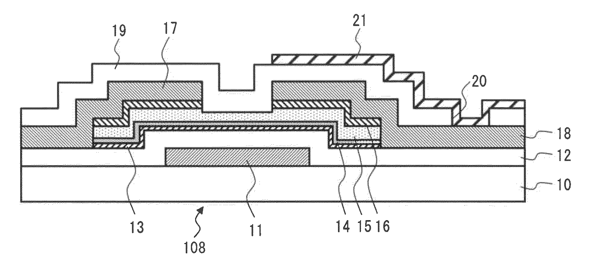
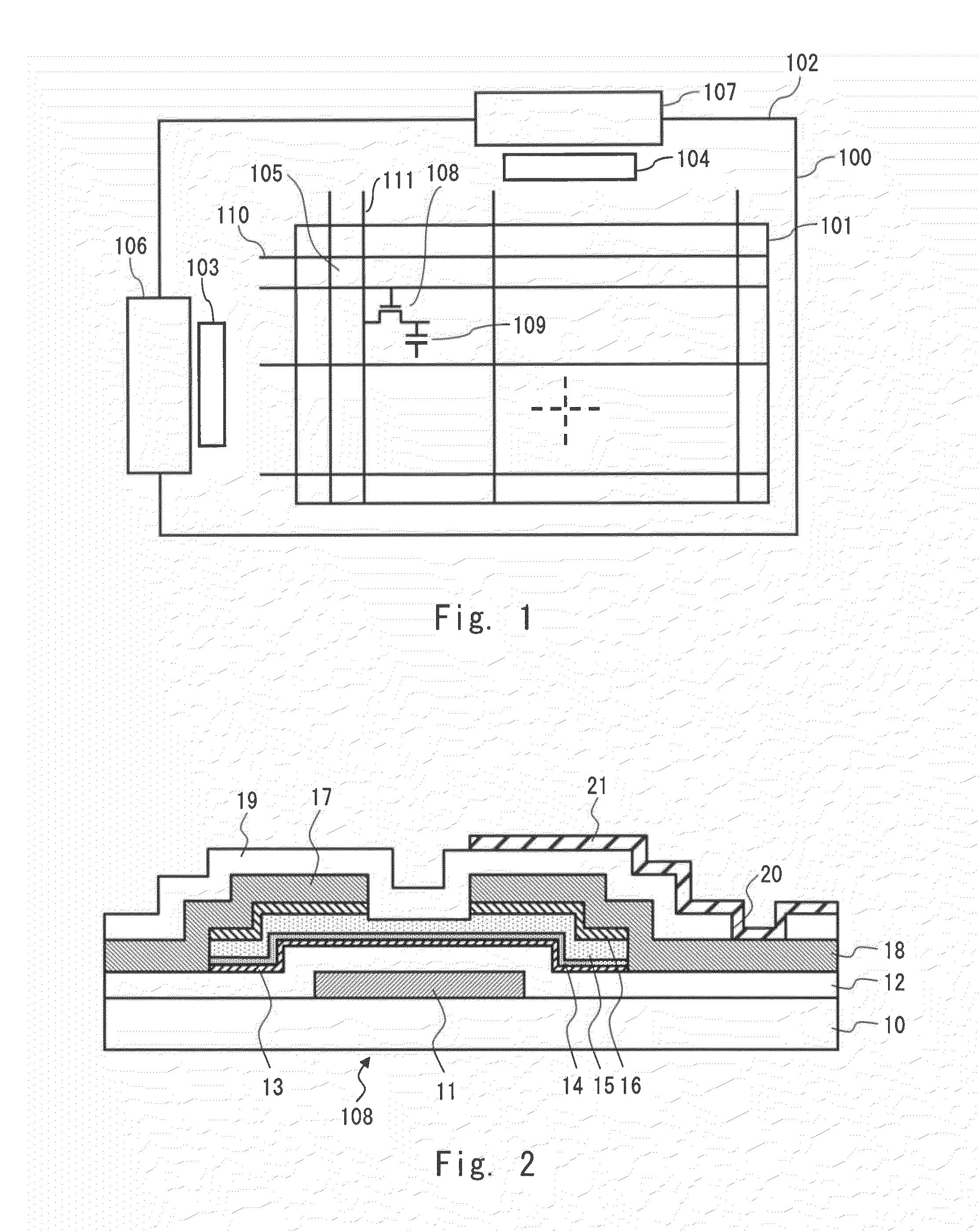
[0029]A TFT substrate that includes a thin-film transistor (TFT) according to an exemplary embodiment of the present invention is described firstly with reference to FIG. 1. FIG. 1 is a schematic front view showing a structure of the TFT substrate. The TFT substrate is used for a display (particularly, an active matrix display), which is a semiconductor device. Although a liquid crystal display is described as an example of the display, it is only by way of illustration. Another flat panel display such as an organic EL display may be used as the display as a matter of course.

[0030]A liquid crystal display includes a TFT substrate 100. The TFT substrate 100 is a TFT array substrate in which TFTs 108 are arranged in an array, for example. The TFT substrate 100 includes a display area 101 and a frame area 102 surrounding the display area 101. In the display area 101, a plurality of gate lines (scan signal lines) 110, a plurality of capacitor lines (not shown) and a ...


PUM


Abstract

A back-channel-etch type TFT includes a gate electrode, an SiN film that is formed on the gate electrode, and an SiO film that is formed and patterned on the SiN film. The TFT further includes an polycrystalline semiconductor film that is formed and patterned on the SiO film in contact with the SiO film in such a way that all pattern ends of the polycrystalline semiconductor film are located in close proximity to pattern ends of the SiO film.

Description

INCORPORATION BY REFERENCE[0001]This application is based upon and claims the benefit of priority from Japanese patent application No. 2009-005600, filed on Jan. 14, 2009, the disclosure of which is incorporated herein in its entirety by reference.BACKGROUND OF THE INVENTION[0002]1. Field of the Invention[0003]The present invention relates to a back-channel-etch type thin-film transistor, a semiconductor device and manufacturing methods thereof.[0004]2. Description of Related Art[0005]A liquid crystal display (LCD), which is one of hitherto-used general low-profile panels, is widely used as a monitor of a personal computer, a monitor of a portable information terminal device and so on for its merits such as low power consumption, small size and lightweight. Further, the LCD has recently become widely used in TV applications in place of a cathode ray tube. Furthermore, an electroluminescence (EL) display that has overcome problems such as limitations on viewing angle and contrast whi...

Claims


Application Information

Patent Timeline
Patent Type & Authority Applications(United States)
IPC IPC(8): H01L29/786H01L21/20H01L21/336
CPCH01L21/02532H01L21/02675H01L29/78678H01L29/66765H01L29/78669H01L29/4908
Inventor TAKEGUCHI, TORU
Owner MITSUBISHI ELECTRIC CORP
Why Eureka
Try Eureka