MEMS device and method for manufacturing the same

a technology of mems device and movable portion, which is applied in the direction of microelectromechanical systems, electrical apparatus, microstructural technology, etc., can solve the problems of limited structural dimension accuracy, inability to obtain sufficient device accuracy, and difficulty in forming a mems resonator having accuracy corresponding, so as to improve the performance characteristic of a mems device and reduce the rigidity of the section minimum portion, the performance characteristic of the movable portion becomes smaller

Inactive Publication Date: 2010-07-15
SEIKO EPSON CORP
View PDF14 Cites 15 Cited by
  • Summary
  • Abstract
  • Description
  • Claims
  • Application Information

AI Technical Summary

Benefits of technology

[0008]An advantage of the invention is to provide a structure and a method for manufacturing the structure that can improve a performance characteristic of a MEMS device.
[0009]According to a first aspect of the invention, a micro electro mechanical systems (MEMS) device includes a substrate and a MEMS structure formed on the substrate. In the device, the MEMS structure includes an operation structure including a support portion formed on the substrate and a movable portion that is extended from the support portion and movable above the substrate. The movable portion has a section minimum portion whose a sectional area orthogonal to a direction toward the movable portion from the support portion is smaller than a sectional area of the movable portion. The section minimum portion is formed by a boundary pattern provided to a planar pattern of the operation structure.
[0010]According to the aspect, the section minimum portion formed by the boundary pattern provided to the planar pattern of the movable portion is provided to the movable portion of the operation structure. Thus, the rigidity of the section minimum portion becomes lower than its both sides. As a result, the influence of the structure from the section minimum portion to the support portion side on the performance characteristic of the movable portion becomes smaller. Since the rigidity of the section minimum portion is reduced by the boundary pattern, the structural dimensions that largely influence on the performance characteristic are defined by the pattern accuracy on the planer pattern of the boundary pattern of the movable portion of the operation structure. As a result, it is possible to reduce the influence on the performance characteristic due to errors and variations of the structural dimensions except for the pattern accuracy of the movable portion, enabling the performance accuracy of the MEMS device to be enhanced. Such errors and variations include errors and variations of an extension length of the operation structure caused by a pattern shift, for example.
[0011]For example, in MEMS resonators, the section minimum portion serves as a vibration node when the movable portion is vibrated. Accordingly, the influence by the planer shape of the movable portion is increased while the influence by the structure from the section minimum portion to the support portion side is decreased. Consequently, it is possible to enhance the frequency accuracy.
[0012]In the MEMS device, the boundary pattern may be a notch formed on a side edge of the operation structure. The boundary pattern is formed by the notch provided on the side edge of the operation structure, i.e., on the edge portion of the operation structure extended toward the movable portion from the support portion. As a result, the rigidity of the section minimum portion is easily reduced by changing the shape of the outer edge of the planer pattern.
[0013]Preferably, in the device, the notch is formed on each side edge of the operation structure. The notches formed on each side edge of the operation structure allow the rigidity of the section minimum portion to be further reduced.

Problems solved by technology

As a result, sufficient device accuracy may not be obtained.
However, limits of accuracy in the structural dimensions generally make it hard to form a MEMS resonator having accuracy corresponding to the frequency accuracy of the related art quartz crystal resonator (about several ppm).
Such errors and variations include errors and variations of an extension length of the operation structure caused by a pattern shift, for example.
Accordingly, the boundary pattern can be manufactured without adding complexity to the manufacturing process as well as an increase in the manufacturing costs.

Method used


Image

  • MEMS device and method for manufacturing the same
  • MEMS device and method for manufacturing the same
  • MEMS device and method for manufacturing the same

Examples


first embodiment

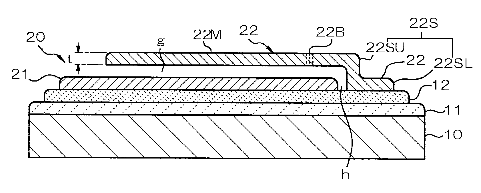
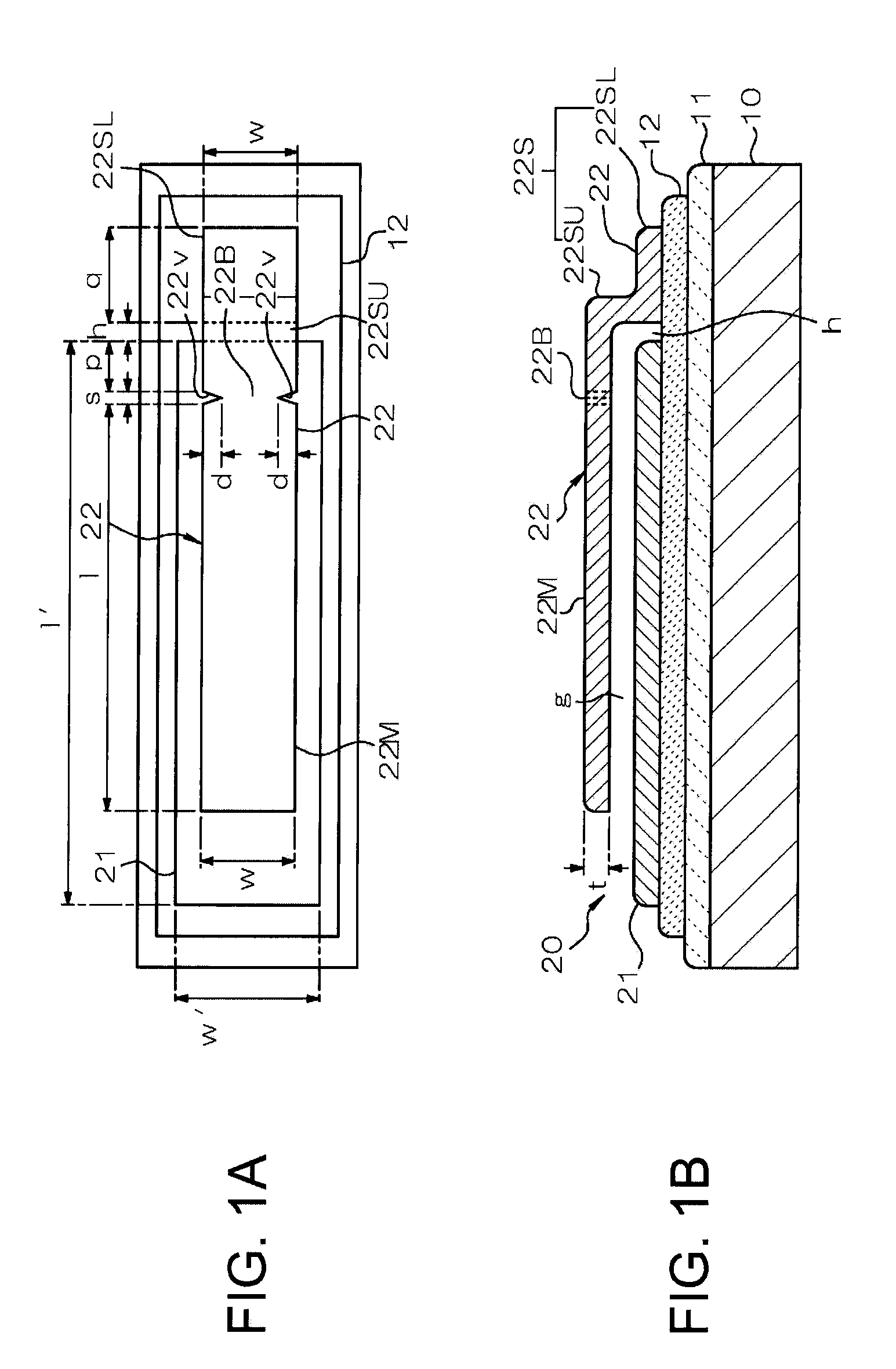
[0037]As shown in FIGS. 1A and 1B, the MEMS device according to the first embodiment includes a MEMS structure 20 formed on a substrate (wafer) 10 serving as a base. The substrate 10 is formed of a semiconductor or the like such as monocrystalline silicon. The substrate 10 is not limited to the semiconductor, and can be formed of various materials such as glass, ceramics, and resin.

second embodiment

[0038]As shown in FIGS. 9A and 9B, an insulation film 11 formed of silicon oxide or the like is formed on a surface of the substrate 10 if necessary, so that the insulation with the substrate 10 is ensured. The insulation film 11 is unnecessary in a case where the substrate 10 is formed of a material having a high insulation property such as glass, ceramics, resin, and a low doped semiconductor, or in a case of using a substrate having an insulation film formed on a surface thereof (e.g., an SOI substrate or the like).

[0039]Formed on the surface of the substrate 10 is a base layer 12 having resistance to an etching process, such as release etching, described below. The base layer 12 is formed of a silicon nitride film formed by a CVD method or the like if a general silicon-based semiconductor manufacturing technique is employed. The base layer 12 is preferably formed in a limited region required in the etching process.

[0040]As shown in FIGS. 10A and 10B, formed on the substrate 10 b...

examples

[0057]FIG. 4 is a graph showing the dependence of resonant frequency of the MEMS device. In the graph, first, second, and third examples are compared with a comparative example.

[0058]In the first example, the l=43 μm, the thickness t=2 μm, the width w=10 μm, the depth d=3 μm, a width s=2 μm, a distance p=5 μm, the space h=2 μm, and a length q=10 μm in the structure shown in FIGS. 1A and 1B where the length l is a length between the end of the movable portion 22M and the boundary position in the end of the notch 22, the depth d is a depth of the notch 22v, the width s is a width of the notch 22v along the side edge, the distance p is a distance between the boundary position in the support 22S side of the notch 22v and the end edge of the lower structure portion 21 in a planar direction, and the length q is a length of the support portion 22S. Here, the length of the movable portion 22M is a length extended from the support portion 22S, i.e., an extension length L=1+s+p+h. The second ...


PUM


Abstract

A micro electro mechanical systems (MEMS) device includes a substrate and a MEMS structure formed on the substrate. In the device, the MEMS structure includes an operation structure including a support portion formed on the substrate and a movable portion that is extended from the support portion and movable above the substrate. The movable portion has a section minimum portion whose a sectional area orthogonal to a direction toward the movable portion from the support portion is smaller than a sectional area of the movable portion located on each side of the section minimum portion. The section minimum portion is formed by a boundary pattern provided to a planar pattern of the operation structure.

Description

BACKGROUND[0001]1. Technical Field[0002]The present invention relates to a MEMS device and a method for manufacturing the same. Particularly, the invention relates to a structure and a manufacturing method that are preferably used for enhancing the frequency accuracy of a MEMS resonator.[0003]2. Related Art[0004]Micro electro mechanical systems (MEMS) are one of techniques for forming microstructures, and include a technique for producing micro electro mechanical systems in a micron-order and products manufactured by the technique. Electronic circuits of a semiconductor chip are formed by stacking thin films of, such as silicon, an oxide film, and metal, on a substrate. Thus, the circuit structure generally has a planer pattern. However, in a case where the MEMS are used as a technique for forming the semiconductor chip, the thin films formed on the substrate is partially separated from the substrate for forming micron-dimensiond plate springs, mirrors, rotation axes, and that like....

Claims


Application Information

Patent Timeline
Patent Type & Authority Applications(United States)
IPC IPC(8): H03H9/02H01L21/3205
CPCB81B3/0078B81B2201/0271H03H9/2457H03H9/02433B81B2203/0118
Inventor KIHARA, RYUJI
Owner SEIKO EPSON CORP
Why Eureka
Try Eureka