Backside illumination semiconductor image sensor

a semiconductor image sensor and backside illumination technology, applied in semiconductor devices, diodes, radiation control devices, etc., can solve the problems of charge collection, general disturbance of precharge level vsub>rst/sub>, limited useful photoconversion surface area, etc., to improve the collection of charges generated and high charge storage level

Active Publication Date: 2010-08-05
STMICROELECTRONICS (GRENOBLE 2) SAS
View PDF10 Cites 50 Cited by
  • Summary
  • Abstract
  • Description
  • Claims
  • Application Information

AI Technical Summary

Benefits of technology

[0020]An object of embodiments of the present invention is to provide an image sensor which improves the collection of charges generated in t

Problems solved by technology

Precharge level VRST is generally disturbed by noise essentially originating from the thermal noise of the channel of the precharge transistor.
This poses various problems and backside illumination (BSI) devices have been provided in which the device is thinned down on its rear surface side and used so that the light reaches the photodiodes from this rear surface, that is, from the side opposite to the side on which the interconnect stack is formed.
Thus, the useful photoconversion surface area is limited by the surface area necessary to position the transfer

Method used


Image

  • Backside illumination semiconductor image sensor
  • Backside illumination semiconductor image sensor
  • Backside illumination semiconductor image sensor

Examples


second embodiment

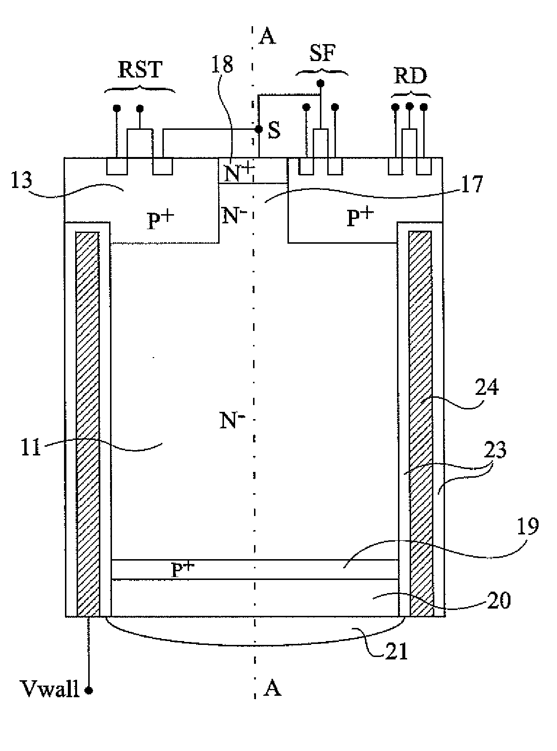
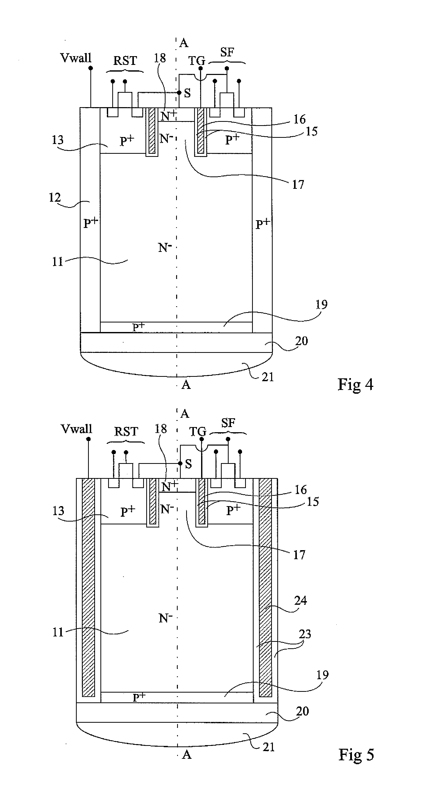
[0044]FIG. 5 is a cross-section view of an image sensor cell. In FIG. 5, the same elements are designated with the same reference numerals as in FIG. 4. The main difference between the cells of FIGS. 5 and 4 is that the insulating wall surrounding the cell is formed of a trench filled with a conductor 24 surrounded with an insulator 23 instead of being a P-type region. Conductor 24 is connected to a terminal Vwall.

[0045]The cells of FIGS. 4 and 5 operate similarly. In both cases, a phase of photoconversion or integration during which the rear surfaces are illuminated and electrons are stored in body 11 is distinguished from a transfer phase during which the electrons are transferred from body 11 to layer 18 and to read node S.

[0046]During the integration phase, the conduction between semiconductor body 11 and heavily-doped N-type region 18 is interrupted by an action on control terminal TG coupled to insulated conductive region 16. Indeed, if electrode TG is set to a negative voltag...

third embodiment

[0053]FIGS. 7 and 8 show two variations of a The embodiment of FIG. 7 is similar to that of FIG. 5 and the same elements have been designated with the same reference numerals. The main difference is that in the embodiment of FIG. 7, grid 15-16 for closing the neck is absent. In this embodiment, during the integration phase, terminal Vwall is set to a strongly positive voltage to create a potential well in body region 11 and thus store the electrons within insulating walls 23. In a plane perpendicular to axis A-A, the electrostatic voltage of body region 11 is maximum along axis A-A and minimum at the level of insulating walls 23. The electrostatic voltage of P+ layer 19 is controlled by the amount of holes stored in this area. For a voltage of layer 19 smaller than the voltage at the level of walls 23, it is possible to store holes. This lack of holes will be compensated by addition of holes originating from the photocurrents. For a layer voltage 19 which tends to be greater than t...


PUM


Abstract

A backside illumination semiconductor image sensor, wherein each photodetection cell includes a semiconductor body of a first conductivity type of a first doping level delimited by an insulation wall, electron-hole pairs being capable in said body after a backside illumination; on the front surface side of said body, a ring-shaped well of the second conductivity type, this well delimiting a substantially central region having its upper portion of the first conductivity type of a second doping level greater than the first doping level; and means for controlling the transfer of charge carriers from said body to said upper portion.

Description

CROSS REFERENCE TO RELATED APPLICATIONS[0001]This application claims the priority benefit of French patent application number 09 / 50723, filed on Feb. 5, 2009, entitled “BACKSIDE ILLUMINATION SEMICONDUCTOR IMAGE SENSOR,” which is hereby incorporated by reference to the maximum extent allowable by law.BACKGROUND OF THE INVENTION[0002]1. Field of the Invention[0003]The present invention relates to a backside illumination semiconductor image sensor.[0004]2. Discussion of the Related Art[0005]FIG. 1 schematically illustrates the circuit of a photosensitive cell of an array of photosensitive cells of an image sensor. A charge transfer transistor TR, a precharge device, and a read device are associated with each photosensitive cell of the array. The precharge device is formed of an N-channel MOS transistor RST, interposed between a supply rail Vdd and a read node S. The read device is formed of the series connection of first and second N-channel MOS transistors SF and RD. The drain of tran...

Claims


Application Information

Patent Timeline
IPC IPC(8): H01L27/148
CPCH01L27/1463H01L27/14632H01L27/14643H01L27/1464H01L27/14689H01L31/112H01L27/14679
Inventor ROY, FRANCOISDESCURE, PATRICK
Owner STMICROELECTRONICS (GRENOBLE 2) SAS
Why Eureka
Try Eureka