Electron emitting element, electron emitting device, light emitting device, image display device, cooling device, and charging device

a technology of electron emitting device and electron emitting element, which is applied in the direction of luminescnet screen, discharge tube, instrument, etc., can solve the problems of ozone damage to human bodies, oxidizing various substances, and breaking down of elements, so as to achieve the effect of reducing the amount of ballistic electrons that transmit the thin-film electrod

Active Publication Date: 2010-08-05
SHARP KK
View PDF38 Cites 21 Cited by
  • Summary
  • Abstract
  • Description
  • Claims
  • Application Information

AI Technical Summary

Benefits of technology

[0019]As described above, the electron emitting element of the present invention has an electron acceleration layer provided between an electrode substrate and a thin-film electrode, which electron acceleration layer includes (a) conductive fine particles and (b) insulating fine particles having an average particle diameter greater than that of the conductive fine particles. Further, the electron emitting element satisfies 0.3x+3.9≦y≦75, where x is the average particle diameter of the insulating fine particles, and y is a thickness of the thin-film electrode.
[0020]According to the configuration, an electron acceleration layer is provided between an electrode substrate and a thin-film electrode, which electron acceleration layer includes (a) conductive fine particles and (b) insulating fine particles having an average particle diameter greater than that of the conductive fine particles. Further, the thin-film electrode has a thickness y (nm) that satisfies the above relational expression. This electron acceleration layer is a thin-film layer in which insulating fine particles and conductive fine particles are minutely assembled, and the electron acceleration layer has a semiconductive property. When a voltage is applied to the semiconductive electron acceleration layer, current flow occurs in the electron acceleration layer. A part of electrons in the current becomes ballistic electrons due to an intense electric field produced by the applied voltage and the ballistic electrons are emitted.
[0021]Here, in order to cause the thin-film electrode to work properly as a planar electrode, the thin-film electrode requires having a thickness of at least 0.3x+3.9 (nm). If the thin-film electrode is thinner than this thickness, electrical conduction cannot be ensured, thereby causing an insufficient flow of current inside the element. Moreover, in order to emit electrons from the electron emitting element through the thin-film electrode, the thin-film electrode requires having a thickness of 75 (nm) or less. If the thickness exceeds 75 nm, the amount of ballistic electrons that transmit the thin-film electrode remarkably decreases. In such a case, the ballistic electrons are absorbed by the thin-film electrode, or alternatively, the ballistic electrons are reflected by the thin-film electrode and are recaptured into the electron acceleration layer. Hence, by specifying the thickness y of the thin-film electrode with the relational expression, it is possible to ensure the electrical conductio

Problems solved by technology

This causes a problem of breakdown of the element due to sputtering.
Ozone is harmful to human bodies, and oxidizes various substances because of its strong oxidizing power.
This causes a problem

Method used


Image

  • Electron emitting element, electron emitting device, light emitting device, image display device, cooling device, and charging device
  • Electron emitting element, electron emitting device, light emitting device, image display device, cooling device, and charging device
  • Electron emitting element, electron emitting device, light emitting device, image display device, cooling device, and charging device

Examples


embodiment 1

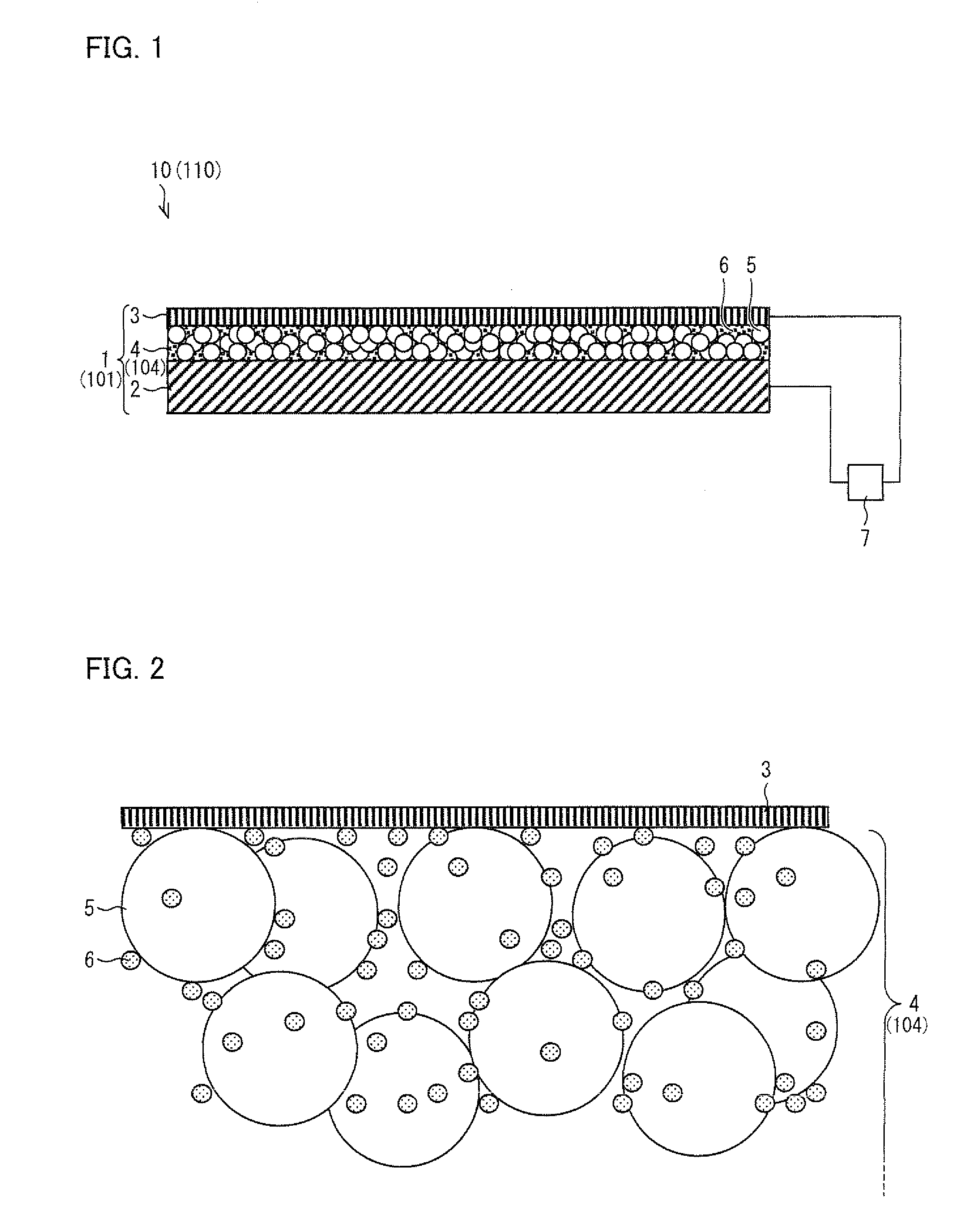
[0047]FIG. 1 illustrates a configuration of an electron emitting device of Embodiment 1 including an electron emitting element according to the present invention. As illustrated in FIG. 1, an electron emitting element 1 of the present embodiment includes an electrode substrate 2 serving as a lower electrode, a thin-film electrode 3 serving as an upper electrode, and an electron acceleration layer 4 sandwiched between the electrode substrate 2 and the thin-film electrode 3. Further, the electrode substrate 2 and the thin-film electrode 3 are connected to a power supply 7, so that a voltage can be applied between the electrode substrate 2 and the thin-film electrode 3 which are provided so as to face each other. The electron emitting element 1 applies a voltage between the electrode substrate 2 and the thin-film electrode 3 so that current flows between the electrode substrate 2 and the thin-film electrode 3, that is, in the electron acceleration layer 4. A part of electrons in the cu...

example of embodiment 1

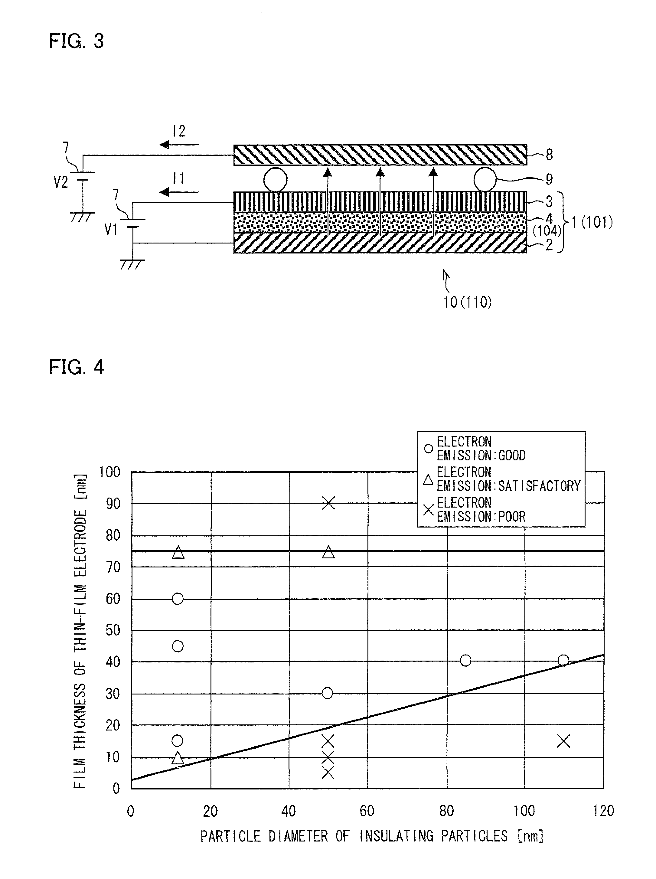
[0069]The present example explains an experiment in which current measurement was carried out by use of electron emitting elements according to Embodiment 1. Note that this experiment is merely an example of the present embodiment and by no means limits the present invention.

[0070]First, electron emitting elements of Examples (Ex.) 1 to 9 and electron emitting elements of Comparative Examples (C. Ex.) 1 to 5 were prepared. The electron emitting elements of Examples 1 to 9 and Comparative Examples 1 to 5 were prepared to have the insulating particles 5 (silica particle diameter) and the thickness of the thin-film electrode 3 (surface electrode film thickness) as shown in Table 1 below. The following description deals with a method for preparing the electron emitting elements of Examples 1 to 9 and Comparative Examples 1 to 5.

[0071]The electron emitting element of Example 1 was prepared as follows. First, 3 mL of hexane solvent was supplied into a 10 mL reagent bottle, and then 0.5 g ...

embodiment 2

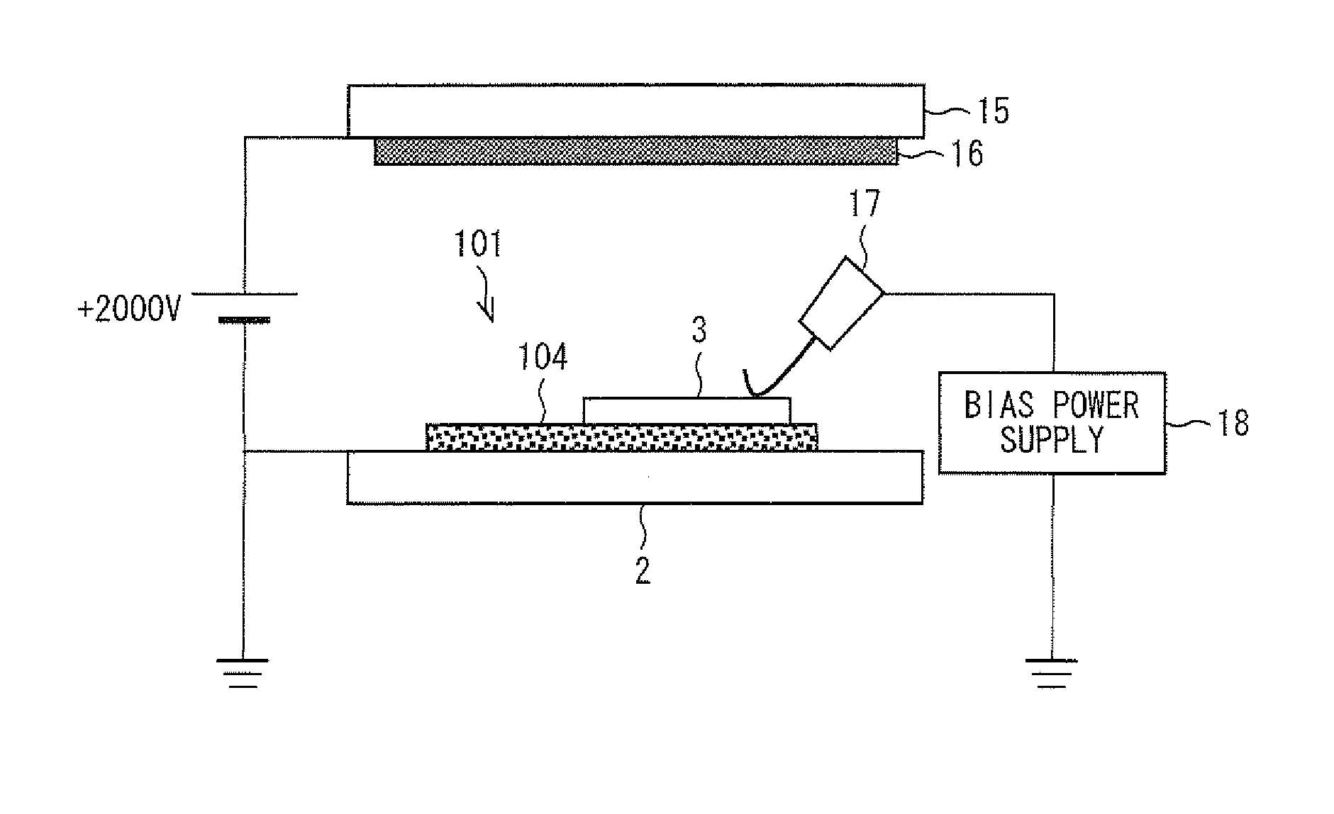
[0084]FIG. 1 illustrates a configuration of an electron emitting device of Embodiment 2, which includes the electron emitting element according to the present invention. As illustrated in FIG. 1, an electron emitting element 101 of the present embodiment includes an electrode substrate 2 serving as a lower electrode, a thin-film electrode 3 serving as an upper electrode, and an electron acceleration layer 104 sandwiched between the electrode substrate 2 and the thin-film electrode 3. Further, the electrode substrate 2 and the thin-film electrode 3 are connected to a power supply 7 so that a voltage can be applied between the electrode substrate 2 and the thin-film electrode 3 which are provided so as to face each other. The electron emitting element 101 and the power supply 7 constitute an electron emitting device 110.

[0085]Note that members that have identical functions to those of members described in Embodiment 1 are given the same reference signs, and the explanations thereof ar...


PUM


Abstract

An electron emitting element of the present invention includes an electron acceleration layer provided between an electrode substrate and a thin-film electrode, which electron acceleration layer includes (a) conductive fine particles and (b) insulating fine particles having an average particle diameter greater than that of the conductive fine particles. The electron emitting element satisfies the following relational expression: 0.3x+3.9≦y≦75, where x (nm) is an average particle diameter of the insulating fine particles, and y (nm) is a thickness of the thin-film electrode 3.
Such a configuration allows modification of the thickness of the thin-film electrode with respect to the size of the insulating particles, thereby ensuring electrical conduction and allowing sufficient current to flow inside the element. As a result, stable emission of ballistic electrons from the thin-film electrode is possible.

Description

[0001]This Nonprovisional application claims priority under 35 U.S.C. §119(a) on Patent Applications No. 2009-024596 filed in Japan on Feb. 5, 2009, and No. 2009-054231 filed in Japan on Mar. 6, 2009, the entire contents of which are hereby incorporated by reference.TECHNICAL FIELD[0002]The present invention relates to an electron emitting element and the like for emitting electrons by application of a voltage.BACKGROUND ART[0003]A Spindt-type electrode and a carbon nanotube electrode (CNT) have been known as conventional electron emitting elements. Applications of such conventional electron emitting elements to, for example, the field of Field Emission Display (FED) have been studied. Such electron emitting elements are caused to emit electrons by tunnel effect resulting from formation of an intense electric field of approximately 1 GV / m that is produced by application of a voltage to a pointed section.[0004]However, each of these two types of the electron emitting elements has an ...

Claims


Application Information

Patent Timeline
IPC IPC(8): G03G15/02H01J1/02H05B41/00H01T23/00H01J9/02
CPCB82Y10/00G03G15/02H01J1/312H05B33/08H01J31/127H01J2201/312H01J2201/3125H01J9/022H05B44/00
Inventor IWAMATSU, TADASHINAGAOKA, AYAEHIRAKAWA, HIROYUKIIMURA, YASUO
Owner SHARP KK
Why Eureka
Try Eureka