Display device with chiplets and light shields

a technology of light shields and display devices, which is applied in the direction of discharge tubes/lamp details, discharge lamps, luminescent screens, etc., can solve the problems of non-uniform electrical performance and visual appearance of displays employing such materials, lower performance compared to conventional transistors made in crystalline silicon wafers, and large thin film transistors (tfts) made from amorphous or polycrystalline silicon are relatively large, so as to achieve enhanced performance and stability of display, and reduce electromagnetic interferen

Active Publication Date: 2010-08-12
GLOBAL OLED TECH
View PDF9 Cites 44 Cited by
  • Summary
  • Abstract
  • Description
  • Claims
  • Application Information

AI Technical Summary

Benefits of technology

[0015]The present invention has the advantage that, by providing first and second light shields with a chiplet-controlled light-emitting diode display, electromagnetic interference is reduced and performance and stability of the display are enhanced.

Problems solved by technology

Thin-film transistors (TFTs) made from amorphous or polycrystalline silicon are relatively large and have lower performance compared to conventional transistors made in crystalline silicon wafers.
Moreover, such thin-film devices typically exhibit local or large-area non-uniformity across the glass substrate that results in non-uniformity in the electrical performance and visual appearance of displays employing such materials.
These changes in current cause non-uniformities in the display, increased or decreased brightness, or other unacceptable display behaviors.
However, these structures can be limited to thin-film circuit designs on substrates.
This arrangement requires that conductive lines or a circuit capacitor be located directly above the TFTs, therefore limits the circuit layout, requires more processing layers than are desirable and might not be useful in other circuit designs and circuit manufacturing processes.
However, there is no teaching of structures or methods for preventing light exposure to circuits in such a pixel-control device.

Method used


Image

  • Display device with chiplets and light shields
  • Display device with chiplets and light shields
  • Display device with chiplets and light shields

Examples


Embodiment Construction

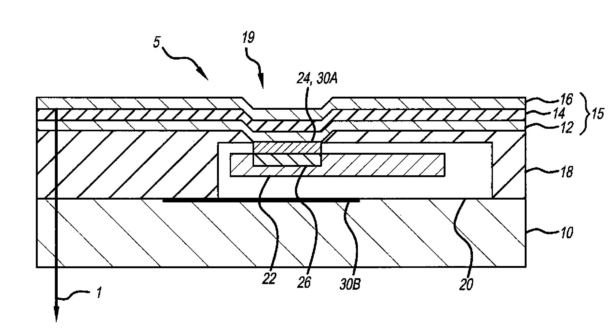
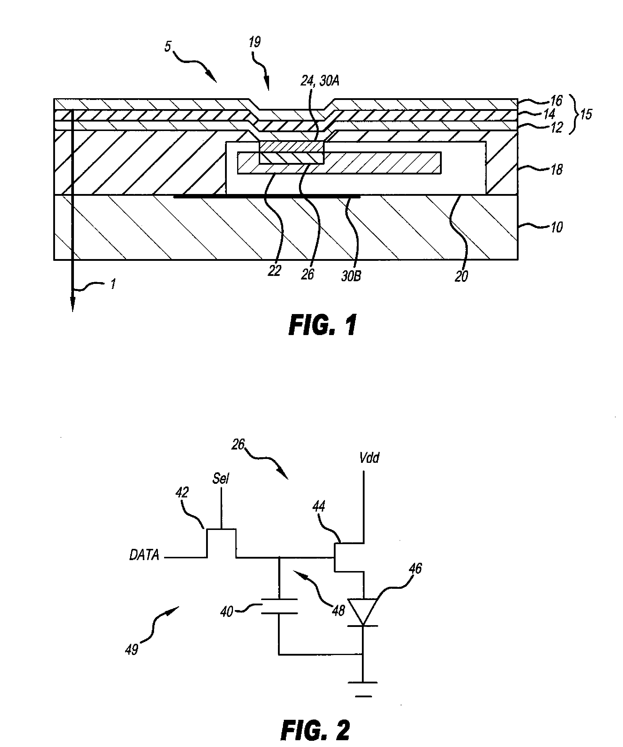
[0025]Referring to FIG. 1, according to one embodiment of the present invention, a light-emitting diode display device includes a transparent substrate 10, a plurality of pixels 5 formed on the transparent substrate 10, each pixel 5 including a transparent electrode 12 formed over the transparent substrate 10, one or more layers 14 of light-emitting material formed over the transparent electrode 12, and a reflective electrode 16 formed over the one or more layers of light-emitting material to from a diode 15 in a bottom-emitter design. In other embodiments of the present invention, the electrode 16 can be transparent and the substrate 10 opaque to provide a top-emitter design. In a design that emits light from both sides of the display, both the electrode 16 and the substrate 10 can be transparent.

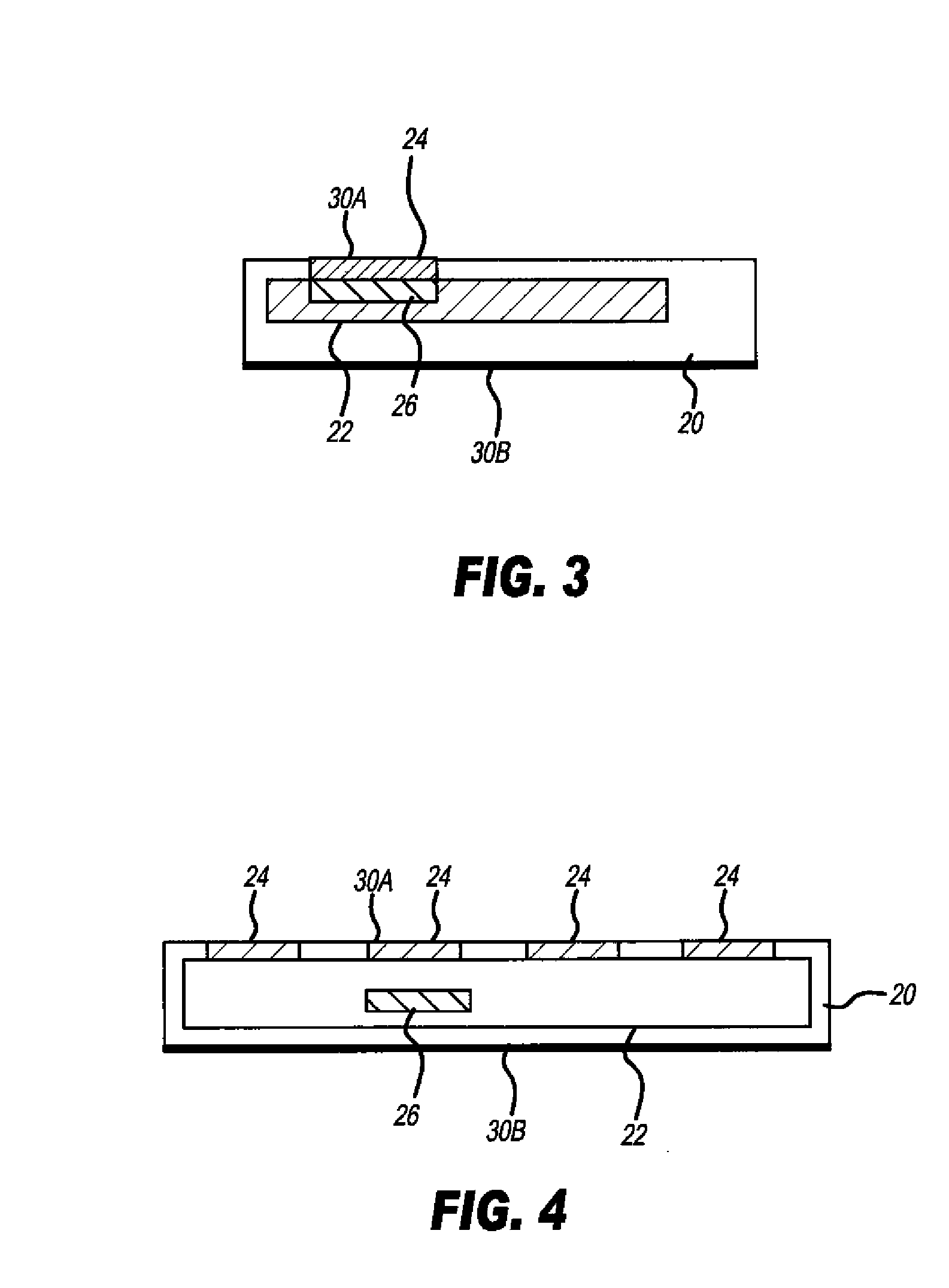
[0026]A plurality of chiplets 20 are located over the transparent substrate 10 between the transparent electrode 12 and the transparent substrate 10, each chiplet 20 including drive circui...


PUM


Abstract

A light-emitting diode display device includes a transparent substrate; a plurality of chiplets located over the substrate between a transparent electrode and the substrate, each chiplet including drive circuitry for driving pixels to emit light and including a storage capacitor for storing charge and wherein light illumination of at least a portion of the drive circuit causes the capacitor to leak charge; a connection pad forming a first light shield separate from the drive circuitry located on the surface of each chiplet disposed over the drive circuitry and substantially shielding at least a portion of the drive circuitry from illumination, the connection pad electrically connected to the drive circuitry, and a second light shield disposed under the drive circuitry between the drive circuitry and the substrate to shield at least a portion of the drive circuitry from illumination.

Description

FIELD OF THE INVENTION[0001]The present invention relates to display devices having a substrate with distributed, independent chiplets for controlling a pixel array.BACKGROUND OF THE INVENTION[0002]Flat-panel display devices are widely used in conjunction with computing devices, in portable devices, and for entertainment devices such as televisions. Such displays typically employ a plurality of pixels distributed over a substrate to display images. Each pixel incorporates several, differently colored light-emitting elements commonly referred to as sub-pixels, typically emitting red, green, and blue light, to represent each image element. As used herein, pixels and sub-pixels are not distinguished and refer to a single light-emitting element. A variety of flat-panel display technologies are known, for example plasma displays, liquid crystal displays, and light-emitting diode (LED) displays.[0003]Light emitting diodes (LEDs) incorporating in films of light-emitting materials forming l...

Claims


Application Information

Patent Timeline
Patent Type & Authority Applications(United States)
IPC IPC(8): H01J1/62
CPCH01L27/3248H01L27/3272H01L27/3255H10K59/129H10K59/123H10K59/126H10K59/00
Inventor COK, RONALD S.PARRETT, GARY J.
Owner GLOBAL OLED TECH
Why Eureka
Try Eureka