Diffraction order sorting filter for optical metrology

a filter and optical metrology technology, applied in the field of optical metrology, can solve the problems of unplanned light dispersion, anomalous diffraction signals measured at wavelengths in the vicinity of joints between osf zones, and overlapped diffraction orders generated by gratings

Active Publication Date: 2010-08-12
TOKYO ELECTRON LTD
View PDF9 Cites 16 Cited by
  • Summary
  • Abstract
  • Description
  • Claims
  • Application Information

AI Technical Summary

Benefits of technology

[0014]According to a further embodiment of the invention, a method is provided for wavelength vs. array detector pixel location calibration which can accommodate and correct for dispersion at zone joints in an OSF filter, by utilizing separate calibration curves in the vicinity of zone joints, to accommodate for the highly nonlinear nature of the wavelength to pixel location calibration curve at and / or in the vicinity of zone joints.

Problems solved by technology

However, when the wavelength range of the diffraction signal exceeds one octave, as is typically the case in semiconductor optical metrology systems, the diffraction orders generated by the grating start to overlap each other.
One of the drawbacks of a zoned OSF is the appearance of anomalies in measured diffraction signals at wavelengths in the vicinity of joints between OSF zones.
The sharp change of traversed optical length at the zone joint may cause unwanted dispersion of light, such that light incident at the zone joint is spread sideways onto multiple pixels of the array detector.
In addition to spreading onto multiple adjacent pixels, this dispersion may cause a sideways shift of the centroid of the image projected upon the detector.
The inventors believe this image spreading and shifting to be the main cause of unwanted localized anomalies in the measured diffraction signals at the zone joints.

Method used


Image

  • Diffraction order sorting filter for optical metrology
  • Diffraction order sorting filter for optical metrology
  • Diffraction order sorting filter for optical metrology

Examples


embodiment 800

[0054]FIG. 8 shows an embodiment 800 of, for example, order sorting filter (OSF) 570 of FIG. 5. OSF 800 has three zones, whose passbands are determined by thin-film stack filters 820A, 820B, and 820C respectively, all deposited on a common optically-transparent substrate 810. The optically-transparent substrate 810 can be made of DUV grade silica, to allow for high transmission in the UV and DUV parts of the spectrum, but other materials can also be used, such as various types of glass, quartz, calcium-fluoride, sapphire, etc. An antireflective coating 840 may be applied to the side of optically-transparent substrate opposite the thin-film stack filters 820A, 820B, and 820C, to minimize light reflections at the substrate-to-air interface. Thin-film stack filters 820A, 820B, and 820C are made of multiple thin films, whose thicknesses and materials determine their passband.

[0055]The process of designing thin-film stack filters given a set of known passband requirements and other const...

embodiment 900

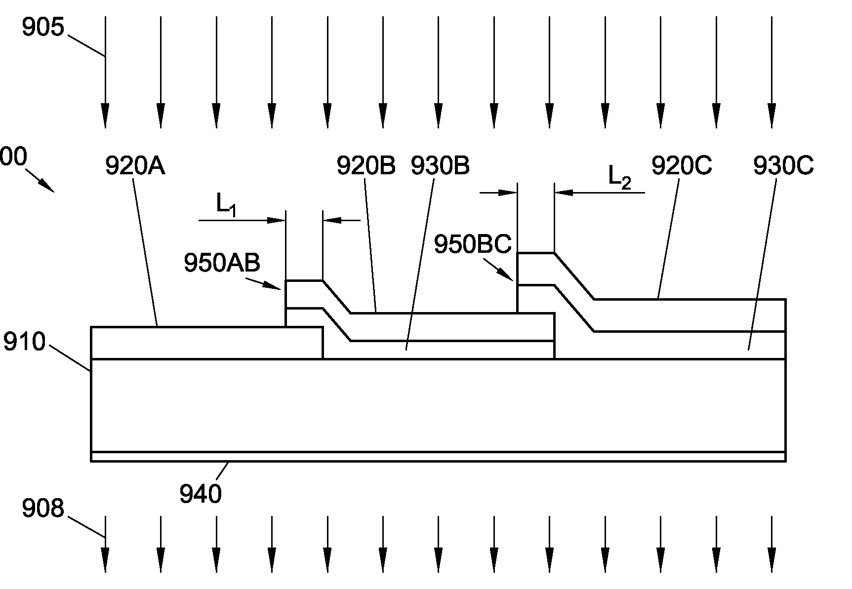
[0059]FIG. 9 shows an embodiment 900 of, for example, order sorting filter (OSF) 570 of FIG. 5. OSF 900 has three zones, whose passbands are determined by thin-film stack filters 920A, 920B, and 920C respectively, all deposited on a common optically-transparent substrate 910. The optically-transparent substrate 910 can be made of DUV grade silica, to allow for high transmission in the UV and DUV parts of the spectrum, but other materials can also be used, such as various types of glass, quartz, calcium-fluoride, sapphire, etc. An antireflective coating 940 may be applied to the side of optically-transparent substrate opposite the thin-film stack filters 920A, 920B, and 920C, to minimize light reflections at the substrate-to-air interface. Thin-film stack filters 920A, 920B, and 920C are made of multiple thin films, whose thicknesses and materials determine their passband.

[0060]Incident light beam 905 is transmitted through thin-film stack filters 920A, 920B, 920C, the optically-tran...

embodiment 1000

[0063]FIG. 10 shows an embodiment 1000 of, for example, order sorting filter (OSF) 570 of FIG. 5. OSF 1000 has three zones, of which the first one does not have a thin-film stack filter deposited thereupon. The passbands of the remaining two zones are determined by thin-film stack filters 1020B and 1020C respectively, all deposited on a common optically-transparent substrate 1010. The optically-transparent substrate 1010 can be made of DUV grade silica, to allow for high transmission in the UV and DUV parts of the spectrum, but other materials can also be used, such as various types of glass, quartz, calcium-fluoride, sapphire, etc. An antireflective coating 1040 may be applied to the side of optically-transparent substrate opposite the thin-film stack filters 1020B and 1020C, to minimize light reflections at the substrate-to-air interface. Thin-film stack filters 1020B and 1020C are made of multiple thin films, whose thicknesses and materials determine their passband.

[0064]Incident...


PUM


Abstract

A zoned order sorting filter for a spectrometer in a semiconductor metrology system is disclosed with reduced light dispersion at the zone joints. The order sorting filter comprises optically-transparent layers deposited underneath, or on top of thin-film filter stacks of the order sorting filter zones, wherein the thicknesses of the optically-transparent layers are adjusted such that the total optical lengths traversed by light at a zone joint are substantially equal in zones adjacent the zone joint. A method for wavelength to detector array pixel location calibration of spectrometers is also disclosed, capable of accurately representing the highly localized nonlinearities of the calibration curve in the vicinity of zone joints of an order sorting filter.

Description

CROSS-REFERENCE TO RELATED APPLICATIONS[0001]This application is related to co-pending U.S. patent application Ser. No. 12 / ______, entitled “CALIBRATION METHOD FOR OPTICAL METROLOGY” (Ref. No. TTI-219), filed on even date herewith, the entire contents of which are herein incorporated by reference in their entirety.BACKGROUND OF THE INVENTION[0002]1. Field of the Invention[0003]This invention relates to optical metrology used in the manufacturing of semiconductor devices, and more particularly to a zoned diffraction order sorting filter for spectrometers used in semiconductor optical metrology systems, and to a method for wavelength calibration of spectrometers with zoned order sorting filters.[0004]2. Description of Related Art[0005]One type of optical metrology involves directing an incident beam at a structure on a workpiece, measuring the resulting diffraction signal, and analyzing the measured diffraction signal to determine various characteristics of the structure. The workpiec...

Claims


Application Information

Patent Timeline
Patent Type & Authority Applications(United States)
IPC IPC(8): G02B27/44G02B27/42
CPCG01B2210/56G01J3/02G01J3/0229G02B2207/117G01J3/18G01J3/28G02B5/28G01J3/0297
Inventor NORTON, ADAMTUITJE, HOLGERSTANKE, FRED
Owner TOKYO ELECTRON LTD
Why Eureka
Try Eureka