
Semiconductor memory device having a discharge path generator for global I/O lines

a memory device and global i/o technology, applied in the field of data path circuits of semiconductor memory devices, can solve problems such as data stored in advance in the selected memory cell to be affected, data loss, and data loss, and achieve the effect of minimizing or eliminating problems

Active Publication Date: 2010-08-12
SAMSUNG ELECTRONICS CO LTD
View PDF5 Cites 5 Cited by
  • Summary
  • Abstract
  • Description
  • Claims
  • Application Information

AI Technical Summary

Benefits of technology

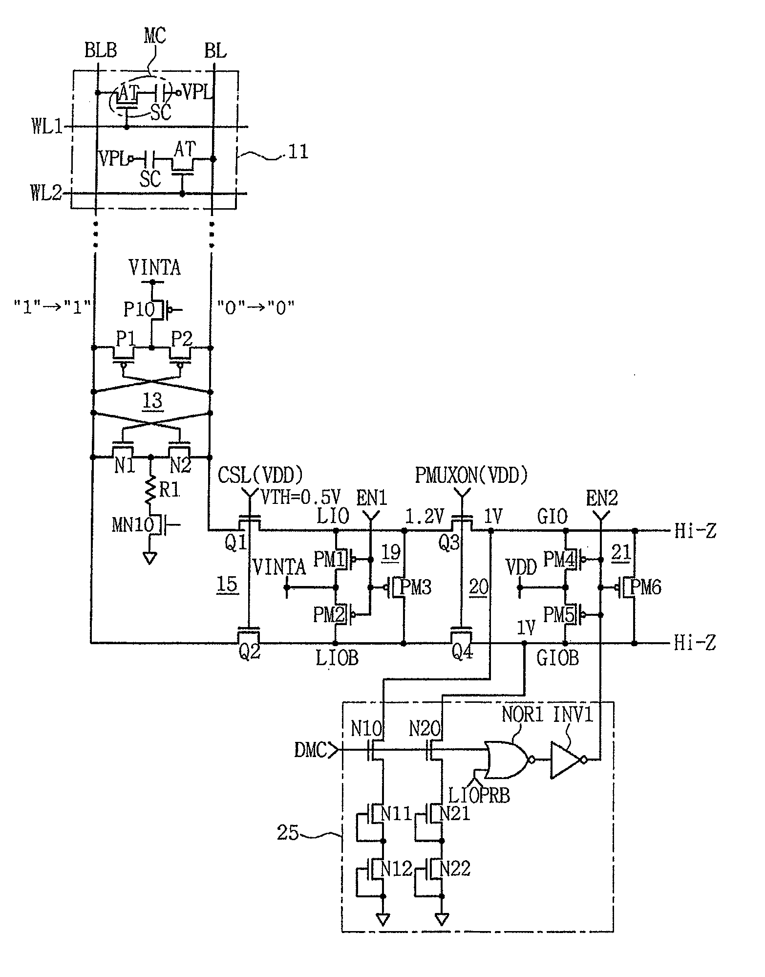
[0011]Exemplary embodiments of the inventive concept provide a semiconductor memory device capable of minimizing or eliminating a problem regarding bit line disturbance during a data masking operation mode while a write operation is being executed.
[0012]Exemplary embodiments of the inventive concept provide a data path circuit for a semiconductor memory device capable of allowing a data masking operation to be reliably performed.
[0013]Exemplary embodiments of the inventive concept provide a precharge scheme for global input / output lines capable of minimizing bit line disturbance and also allowing a low-voltage high-speed operation for a high-speed semiconductor memory.

Problems solved by technology

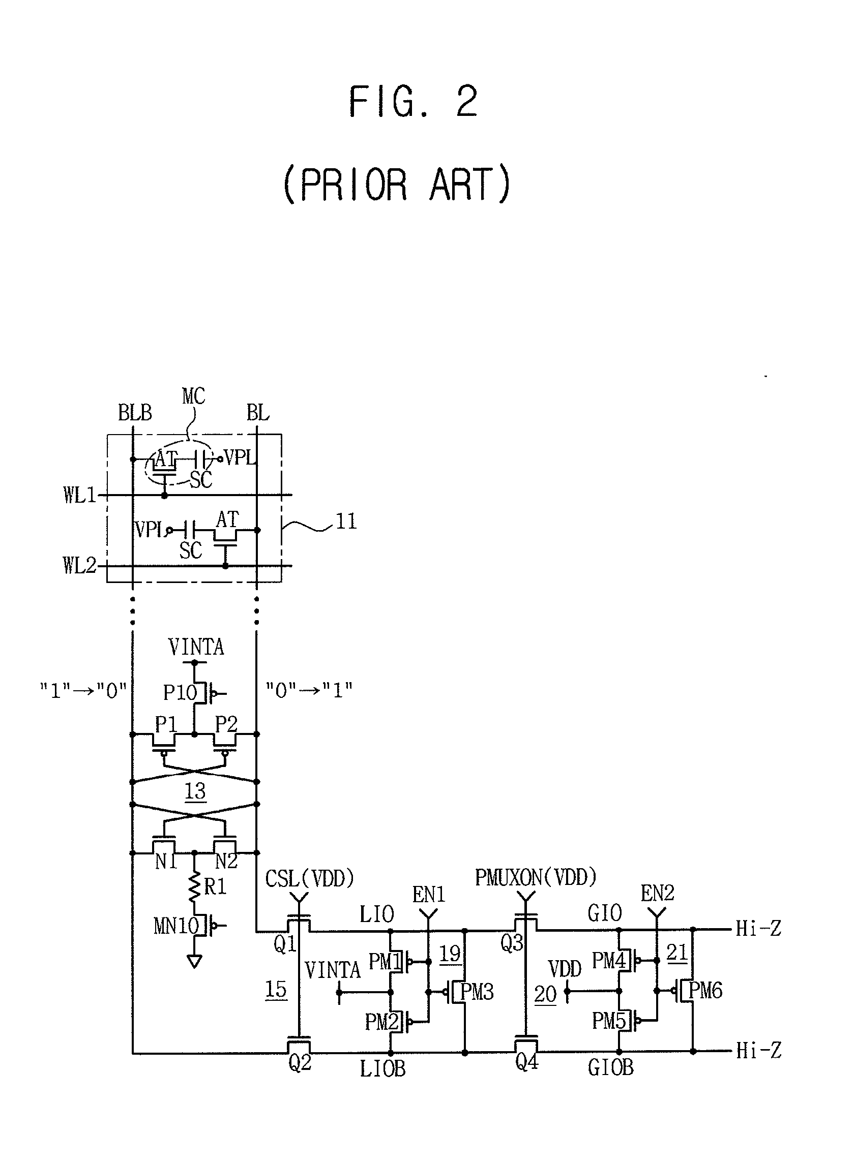
During the data masking operation mode while the write operation is being executed, the electric charges on the global input / output lines may be applied to the bit line connected to the relevant memory cell, which can cause bit line disturbance.
The bit line disturbance can cause data stored in advance in the selected memory cell to be affected, such that a read error can occur during the data read operation.

Method used


Image

  • Semiconductor memory device having a discharge path generator for global I/O lines
  • Semiconductor memory device having a discharge path generator for global I/O lines
  • Semiconductor memory device having a discharge path generator for global I/O lines

Examples


Embodiment Construction

[0034]Exemplary embodiments of the inventive concept are shown by way of example in the drawings and will herein be described below in detail. Like numbers refer to like elements throughout the description of the figures. However, the configuration and basic operation of the typical DRAM or its internal circuits are well known to those skilled in the art and will not be described in further detail.

[0035]It should be understood, however, that there is no intent to limit the exemplary embodiments to the particular forms disclosed, but on the contrary, can include all modifications, equivalents, and alternatives falling within the scope of the inventive concept.

[0036]It will be understood that, although the terms first, second and third may be used herein to describe various elements, these elements should not be limited by these terms. These terms are only used to distinguish one element from another. For example, a first element could be termed a second element, and, similarly, a sec...


PUM


Abstract

A data path circuit includes a bit line sense amplifier, a local input / output line precharger connected to a local input / output line pair, a global input / output line precharger connected to a global input / output line pair, a column selector connecting a bit line pair connected to the bit line sense amplifier and the local input / output line pair to each other in response to a column selection signal, and a local input / output line selector connecting the local input / output line pair and the global input / output line pair to each other in response to a multiplexing control signal. A discharge path generator decreases the potential on the global input / output line pair down to a predetermined level in response to a data masking control signal which is activated earlier than the column selection signal during a data masking operation mode.

Description

CROSS-REFERENCE TO RELATED APPLICATION[0001]This application claims priority to and the benefit of Korean Patent Application 10-2009-0011120, filed on Feb. 11, 2009, in the Korean Intellectual Property Office, the entire content of which is incorporated by reference herein.BACKGROUND[0002]1. Technical Field[0003]The present disclosure relates to semiconductor memory devices, and in particular, to a data path circuit for a semiconductor memory device, such as a dynamic random access memory (DRAM), or the like.[0004]2. Discussion of the Related Art[0005]A DRAM which is often used as a main memory in an electronic system has a high operating speed and is highly integrated according to the users' demands.[0006]Such a DRAM is a volatile memory which has a plurality of memory cells, each typically including one access transistor and one storage capacitor. The DRAM has a refresh operation as well as a read / write operation.[0007]High-performance DRAMs with an improved operating speed, such ...

Claims


Application Information

Patent Timeline
IPC IPC(8): G11C11/24G11C7/00
CPCG11C7/02G11C7/1006G11C11/4096G11C7/1066G11C7/1078G11C7/1048
Inventor JUNG, DAE-HEE
Owner SAMSUNG ELECTRONICS CO LTD
Learn More