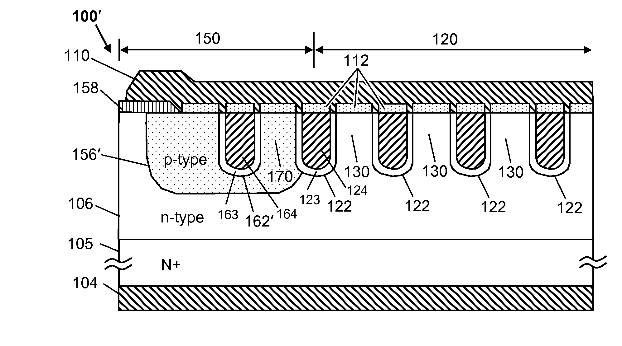
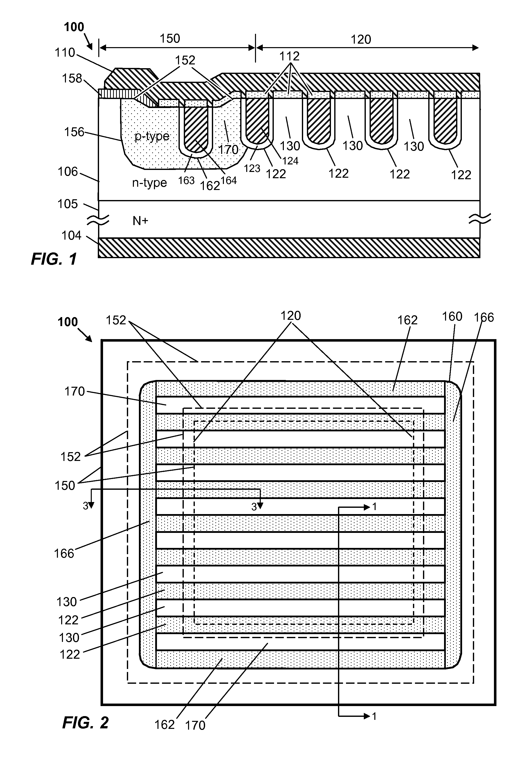
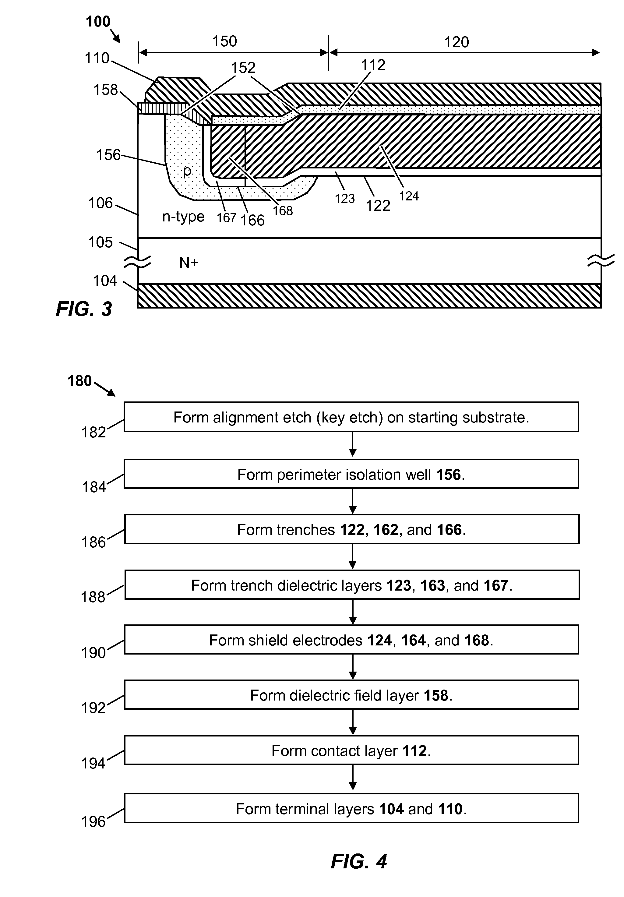
[0004]A first invention of the present application is directed to a trench-shielded
semiconductor device. A first general exemplary embodiment thereof broadly comprises a semiconductor region having a surface; a first area of the semiconductor region; a well region of a first
conductivity type disposed in the semiconductor region and around the first area; and a plurality of trenches extending in a semiconductor region. Each trench has a first end disposed in a first portion of the well region, a second end disposed in a second portion of the well region, and a middle portion between the first and second ends and disposed in the first area. Each trench further has opposing sidewalls lined with a
dielectric layer, and a conductive
electrode disposed on at least a portion of the
dielectric layer. A device region of any suitable and desired type may be disposed between the middle portions of adjacent trenches. The above configuration aids in pushing away
electric potential lines and fields from the device region to increase the
breakdown voltage of the device. Further exemplary embodiments of this invention may include end trenches disposed on either side of the plurality of initially-recited trenches, with each such end trenches being disposed in a respective portion of the well region. Yet further exemplary embodiments may include additional end trenches disposed at the first and second ends of the plurality of initially recited trenches, with each such additional end trenches being disposed in a respective portion of the well region. The above configuration further aids in pushing away
electric potential lines and fields from the device region to increase the
breakdown voltage of the device.
[0005]A second invention of the present application is directed to a method of manufacturing a
semiconductor device with one or more trenches. As part of making this invention, the inventors have discovered that trenches with rounded bottom walls, and with improved quality of the
dielectric layer, can provide improved breakdown voltages. A general exemplary embodiment of this invention comprises: forming one or more initial trenches into a semiconductor region, each trench having a bottom wall and one or more side walls; growing a sacrificial
oxide layer on the walls of the initial trenches; removing the sacrificial
oxide layer; forming a
dielectric layer on the side and bottom walls of the one or more trenches after removing the sacrificial
oxide layer; and filling the one or more trenches with
electrically conductive material. The inventors have found that the growth and removal of the sacrificial oxide rounds the bottom walls of the trenches, and improves the quality of the subsequently formed
dielectric layer by tying up (i.e., resolving) dangling bonds of the etched semiconductor material of the trench walls.
[0006]A third invention of the present application is directed to a method of manufacturing a
semiconductor device with one or more trenches. As part of making this invention, the inventors have found that a conductive bridge can form in the
dielectric layer of the trench that can lead to a breakdown condition, and have found a way to grow a better oxide dielectric
layers that
resist the formation of such conductive bridges. A general exemplary embodiment of this invention comprises: forming one or more trenches into a semiconductor region, each trench having a bottom wall and one or more side walls; growing an oxide layer on the trench bottom and side walls of the one or more trenches at a temperature of 1100° C. or higher in a dry
oxygen environment that is diluted with one or more
inert gases; and filling the one or more trenches with
electrically conductive material. The above conditions of oxide grown, in the context of a trench-shielded power device, provides better a dielectric layer of better quality.
[0008]A fifth invention of the present application is directed to a trench-shielded semiconductor device having p-doped polysilicon trench electrodes. The inventors have discovered that the p-doped polysilicon material enhances the ability of the trench electrodes to shield the mesas of the device from
electric potential lines and fields, and increases the
breakdown voltage of the device. A first exemplary embodiment of this invention is directed to a semiconductor device, the device broadly comprising: a semiconductor region having a surface; and a plurality of trenches extending in a semiconductor region, each trench having a first end, a second end, and a middle portion between the first and second ends, each trench further having opposing sidewalls lined with a dielectric layer, and a conductive
electrode disposed on at least a portion of the dielectric layer, wherein the conductive
electrode comprises p-doped polysilicon. A second exemplary embodiment of this invention is directed to a method of manufacturing a semiconductor device with one or more trenches, the method broadly comprising: forming one or more trenches into a semiconductor region, each trench having a bottom wall and one or more side walls, the one or more trenches defining surfaces of the semiconductor region that are adjacent to the one or more trenches; forming a dielectric layer on the side and bottom walls of the one or more trenches; and filling the one or more trenches with p-doped polysilicon material. The polysilicon may doped by
in situ doping during deposition, by implantation with p-type
dopant after deposition, or by vapor-phase
exposure to p-type
dopant during anneal.


