High voltage semiconductor device

a high-voltage semiconductor and high-voltage technology, applied in the field of high-voltage semiconductor devices, can solve the problems of high process complexity, so-called high-voltage transistors in modern cmos processes, and devices with only limited applicability in high-voltag

Inactive Publication Date: 2010-08-26
NXP BV
View PDF8 Cites 63 Cited by
  • Summary
  • Abstract
  • Description
  • Claims
  • Application Information

AI Technical Summary

Benefits of technology

[0014]The semiconductor device is especially applicable in many CMOS processes, especially in deep submicron CMOS processes. Modern CMOS processes allow mask details, namely in active (STI) and POLY (gate) masks, that can be conveniently exploited for high voltage implementation according to the embodiments of this invention. For example implementation of the present invention in a standard 65 nm CMOS process shows that substantially higher (for example 3 times) extension doping or substantially better active-to-STI width ratio (in the prior invention of applicants) can be used, using said field plates. This enhances the Rds-on versus breakdown Figure of merit substantially (for example up to 2 times).
[0046]The gate-fingers can extend either along a major part of the extended-drain region or along only a small part of the extended-drain region (see FIG. 5a,b). The latter is particularly applicable to reduce hot carrier effects and thus improve device ruggedness and reliability because reduction of the field at the end of the channel at the gate edge is essential for avoidance of hot-carrier effects.

Problems solved by technology

Typically these devices have only limited applicability in high voltage (HV) due to for instance breakdown of voltage.
Integration of such in this respect so-called high voltage transistors in modern CMOS processes is a problem, because typically it cannot be done in a cost-competitive way which would be very attractive.
These implantations results in higher process complexity and higher cost per chip area.
This results in more complex and expensive CMOS process and requires additional process (re-) qualification, which delays introduction of new products in advanced CMOS processes.
Thus, the prior art semiconductor devices are limited in applicability, amongst others due to one or more of problems associated with relatively poor on-resistance vs. breakdown voltage trade-off, high costs due to extra processing steps and / or masks, risks of failure of the device.

Method used


Image

  • High voltage semiconductor device
  • High voltage semiconductor device
  • High voltage semiconductor device

Examples


Embodiment Construction

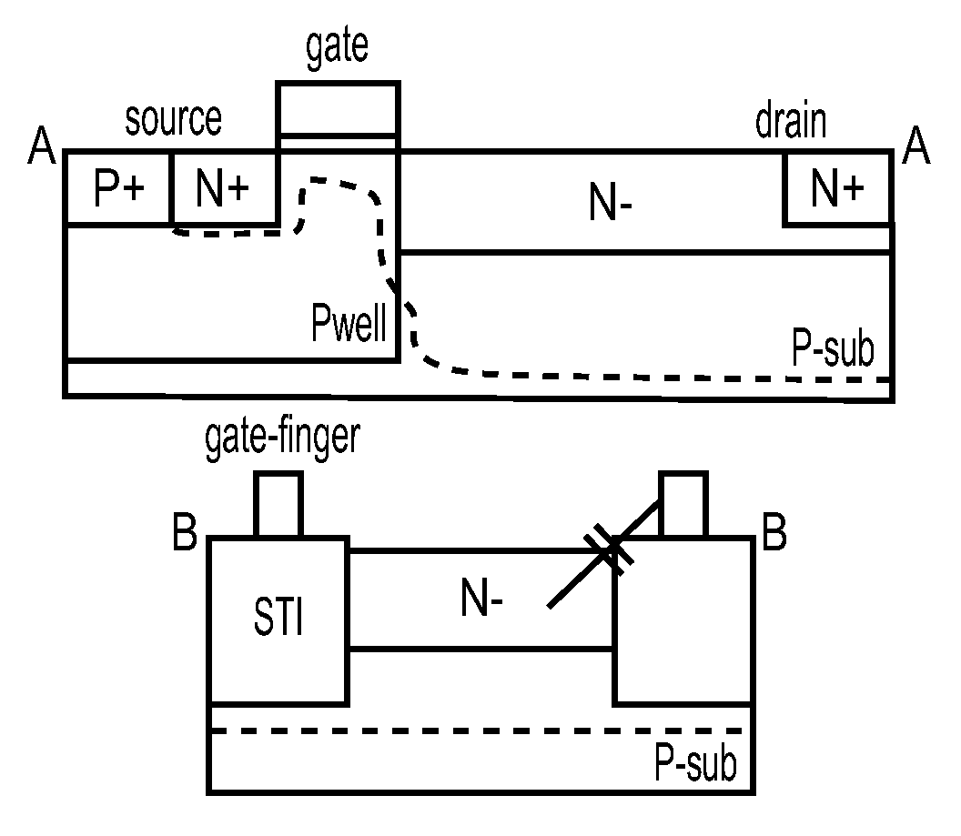
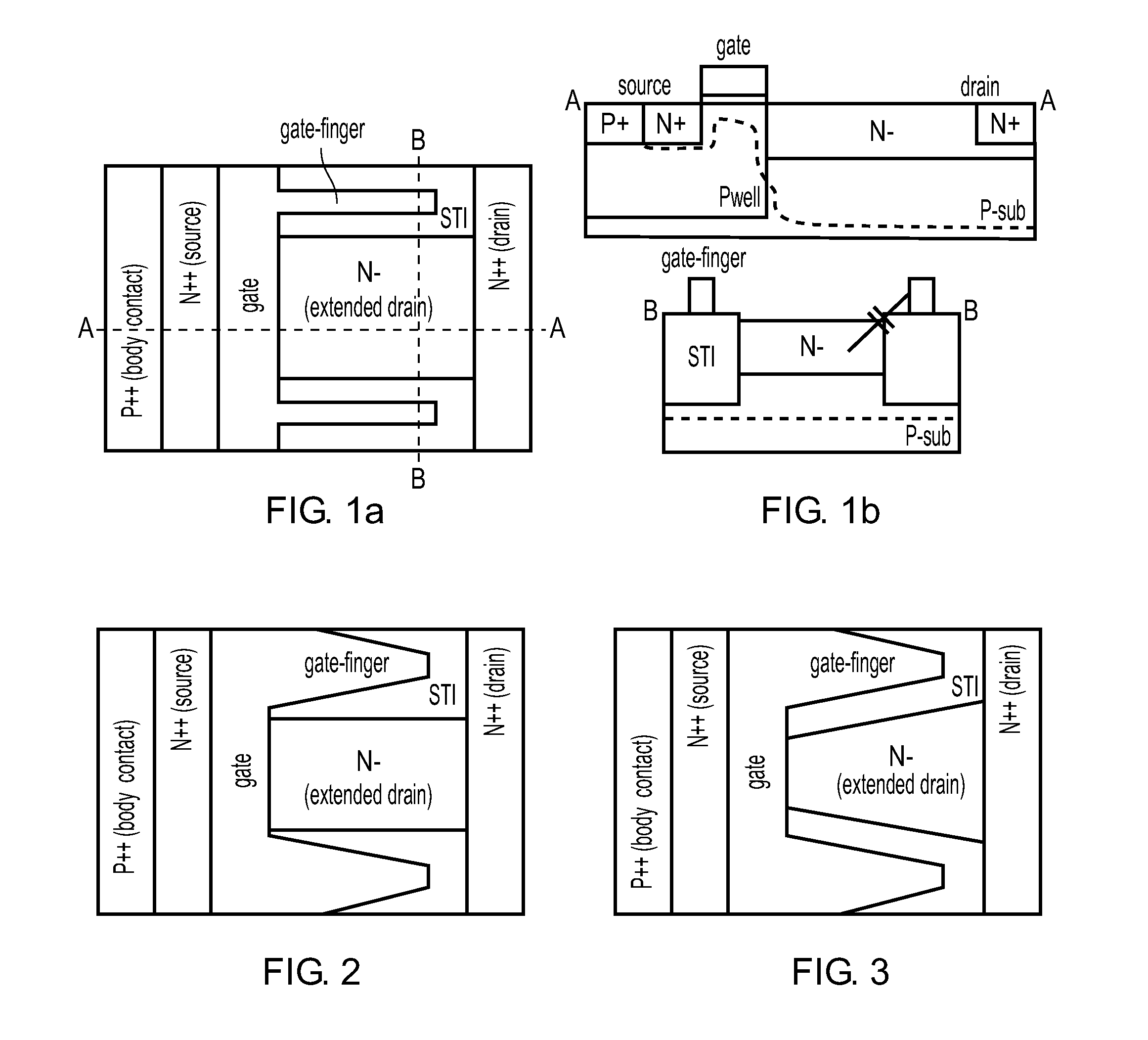
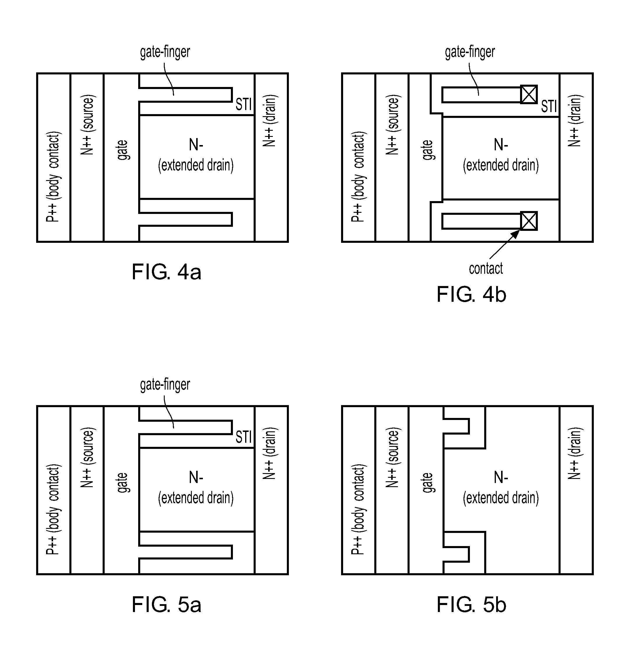
[0012]In a first aspect the present invention relates to a semiconductor device for use in high voltage application, comprising at least one dielectric in substrate region, preferably an STI region, one or more semiconductor regions located between the at least one dielectric region, one or more electrically conductive extensions in a lateral plane, placed on and extending over the at least one dielectric region, wherein the one or more extensions capacitevely interact with the one or more semiconductor regions through a part of the dielectric region between the extension edge and the dielectric edge.

[0013]These conductive extensions are most conveniently realized in IC processes as gate (doped polysilicon) extensions, also called gate fingers, polysilicon fingers, gate field plates or polysilicon field plates in the further description.

[0014]The semiconductor device is especially applicable in many CMOS processes, especially in deep submicron CMOS processes. Modern CMOS processes a...


PUM


Abstract

This invention describes implementation of medium / high voltage semiconductor devices with a better voltage-blocking capability versus specific on-resistanσe trade off. This approach can be implemented in baseline and submicron CMOS without any additional process steps. Said devices comprise dielectric regions and semiconductor regions formed between them. Conductive extentions are formed on the dielectric regions, said extentions interacting capacitively with the semiconducter regions.

Description

FIELD OF THE INVENTION[0001]This invention describes implementation of medium / high voltage semiconductor devices with a better voltage-blocking capability versus specific on-resistance trade off. This approach can be implemented in baseline and submicron CMOS without any additional process steps.BACKGROUND OF THE INVENTION[0002]CMOS semiconductor devices, such as transistors, are known. Typically these devices have only limited applicability in high voltage (HV) due to for instance breakdown of voltage.[0003]Many IC (Integrated Circuit) applications require for instance power management units for DC:DC down- or up-conversion of the supply voltage. Typically NMOS and PMOS semiconductor devices, such as transistors, with capability from 5V up to 25 V are required for such applications.Furthermore, applications such as solid-state lighting, power amplifiers and MEMS sensor or actuator driving circuits require transistors capable of handling voltages up to 50 V or even higher operating ...

Claims


Application Information

Patent Timeline
Patent Type & Authority Applications(United States)
IPC IPC(8): H01L29/78H01L21/762
CPCH01L29/0653H01L29/402H01L29/42356H01L29/42364H01L29/4238H01L29/6609H01L29/861H01L29/66659H01L29/66681H01L29/7816H01L29/7824H01L29/7835H01L29/66325
Inventor SONSKY, JANHERINGA, ANCO
Owner NXP BV
Why Eureka
Try Eureka