Display device and method for controlling the same

a technology of display device and display device, applied in the field of display device and control method, can solve the problems of reducing yield, pixel cannot be pixel, uneven luminance, etc., and achieve the effect of quick and easy detection and correction of uneven luminan

Active Publication Date: 2010-08-26
JOLED INC
View PDF7 Cites 69 Cited by
  • Summary
  • Abstract
  • Description
  • Claims
  • Application Information

AI Technical Summary

Benefits of technology

[0020]Using a display device or a method for controlling the display device according to the present invention allows measurement of a test voltage for characteristics of driving transistors even with simple circuitry, and using the test voltage allows quick and easy detection of a drain current of th...

Problems solved by technology

However, a problem of unevenness in luminance occurs in the active-matrix organic EL display because luminances are different among pixels due to a variation in characteristics of driving transistors or organic EL elements even when the same data signals are provided.
Using complicated pixel circuitry, however, reduces yields.
Feedback compensation using a representative pixel or the sum of currents flowing in all the pixels cannot compensate unevenness in characteristics among pixels.
However, a drive current flowing in pixels is so fine that it is difficult to accurately measure such a fine current via a line, such as a test line, for measuring the current.
For the substrate for a luminescent panel, the method for testing the substrate for the luminescent panel, and the luminescent panel disclosed in the Patent Reference 1, accuracy in detection of characteristics of the driving transistor is poor bec...

Method used


Image

  • Display device and method for controlling the same
  • Display device and method for controlling the same
  • Display device and method for controlling the same

Examples


first embodiment

[0070]A first embodiment of the present invention is hereinafter described with reference to the drawings.

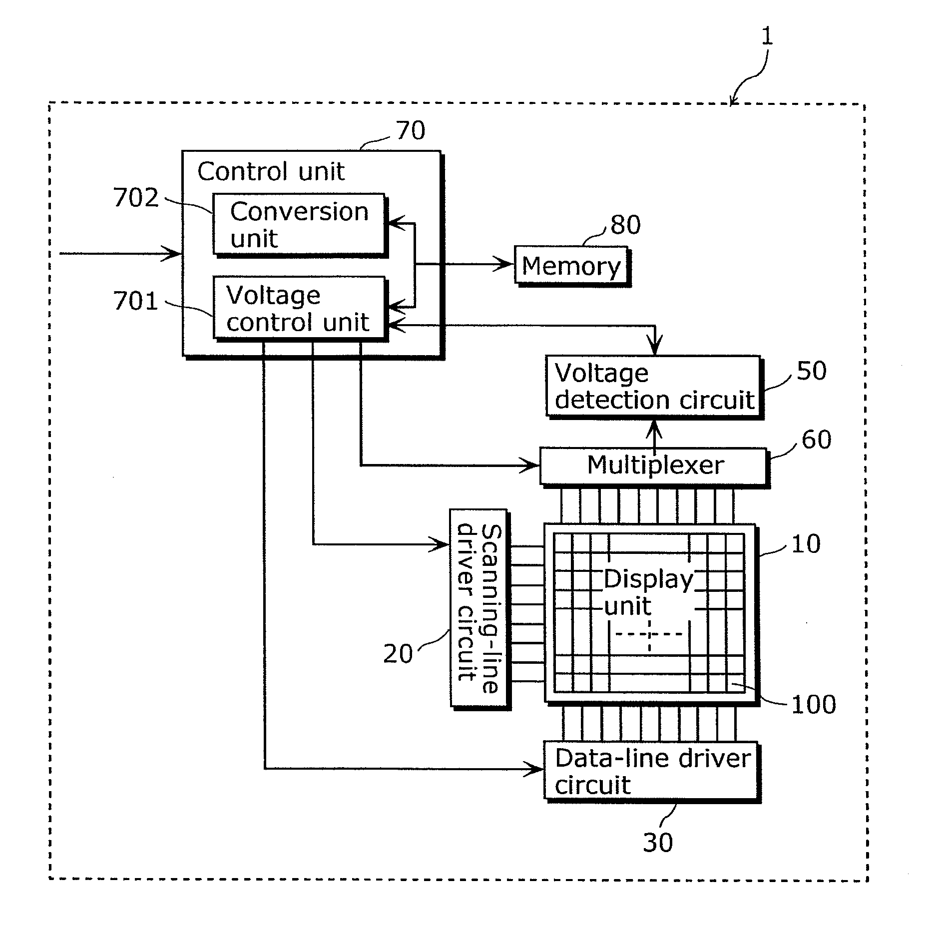
[0071]FIG. 1 is a block diagram which shows an electrical configuration of a display device according to a first embodiment of the present invention. The display device 1 includes a display unit 10, a scanning-line driver circuit 20, a data-line driver circuit 30, a voltage detection circuit 50, a multiplexer 60, a control unit 70, and a memory 80.

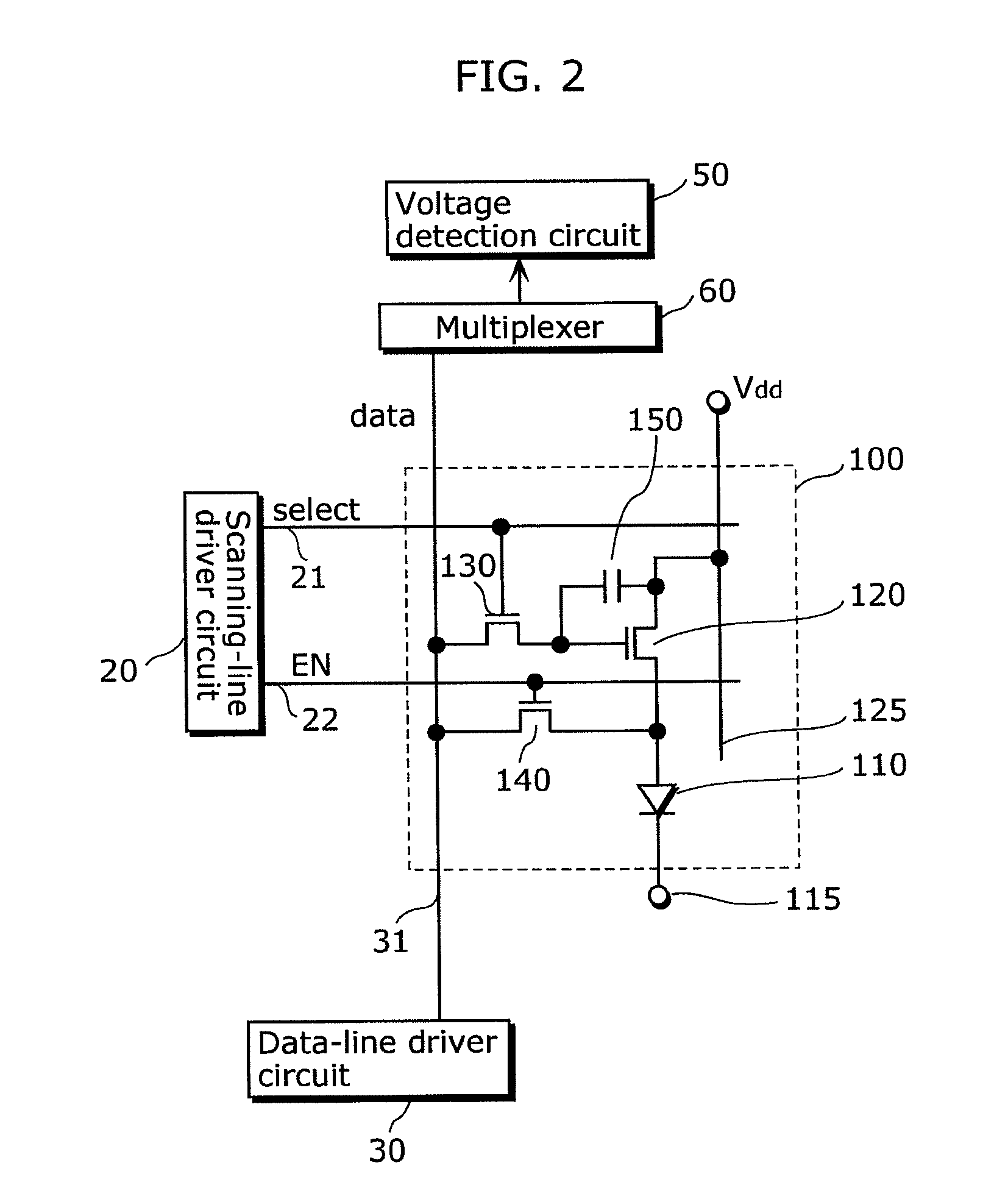
[0072]FIG. 2 is a diagram which shows a circuitry configuration of a pixel unit of the display device according to the first embodiment of the present invention, and connection of the pixel unit with peripheral circuitry thereof. A pixel unit 100 in FIG. 2 includes an organic EL element 110, a driving transistor 120, a switching transistor 130, a test transistor 140, a capacitance element 150, a common electrode 115, a power line 125, a scanning line 21, a control line 22, and a data line 31. The peripheral circuitry includes the scann...

second embodiment

[0141]A second embodiment of the present invention is hereinafter described with reference to the drawings.

[0142]FIG. 11 is a diagram which shows a circuitry configuration of a pixel unit of the display device according to the second embodiment of the present invention, and connection of the pixel unit with peripheral circuitry thereof. A pixel unit 101 in FIG. 11 includes an organic EL element 110, a driving transistor 120, a switching transistor 130, a test transistor 160, a capacitance element 150, a common electrode 115, a power line 125, a scanning line 21, a control line 22, a data line 31, and a read line 53. The peripheral circuitry includes a scanning-line driver circuit 20, a data-line driver circuit 30, a voltage detection circuit 50, a multiplexer 60, and a voltage selection switch 65. Compared to the display device according to the first embodiment, a display device according to the second embodiment of the present invention is different in a configuration in which a re...


PUM


Abstract

A display device includes an organic EL element and a capacitor. A driving transistor is connected to an anode of the organic EL element and passes a current to the organic EL element. The current corresponds to a voltage held in the capacitor. A first switch is between the capacitor and a data line, and the data line supplies the voltage to the capacitor. A voltage detector is connected to the data line for detecting an anode voltage applied to the organic EL element. A second switch is between the anode and the data line. A controller turns on the first switch, causes the organic EL element to emit light, and causes the voltage detector to detect the anode voltage by turning off the first switch and turning on the second switch while the organic EL element is emitting light.

Description

CROSS REFERENCE TO RELATED APPLICATION[0001]This is a continuation application of PCT Application No. PCT / JP2009 / 003023 filed Jun. 30, 2009, designating the United States of America, the disclosure of which, including the specification, drawings, and claims, is incorporated herein by reference in its entirety.[0002]The disclosure of Japanese Patent Application No. 2008-176243 filed on Jul. 4, 2008 including specification, drawings and claims is incorporated herein by reference in its entirety.BACKGROUND OF THE INVENTION[0003]1. Field of the Invention[0004]The present invention relates to display devices and methods for controlling the same, and in particular, to a method for detecting a variation in characteristics of semiconductor driving active elements.[0005]2. Description of the Related Art[0006]Image display devices in which organic EL elements (also known as organic light emitting diodes, or OLEDs) are used, that is, organic EL displays are known as image display devices with ...

Claims


Application Information

Patent Timeline
IPC IPC(8): G06F3/038
CPCG09G3/006G09G3/3233G09G2300/0842G09G3/30G09G2320/043G09G2320/045G09G2330/12G09G2320/0295G09G3/3208H10K2102/301
Inventor SHIROUZU, HIROSHINAKAMURA, TETSUROU
Owner JOLED INC
Why Eureka
Try Eureka