Mosfet, method of fabricating the same, cmosfet, and method of fabricating the same

Inactive Publication Date: 2010-09-02
RENESAS ELECTRONICS CORP
View PDF10 Cites 8 Cited by
  • Summary
  • Abstract
  • Description
  • Claims
  • Application Information

AI Technical Summary

Benefits of technology

[0019]In view of the above-mentioned problems, it is an exemplary object of the present invention to provide an NMOSFET and a method of fabricating the same, both of which are capable of reducing a threshold voltage of an NMOSFET to about ±0.1 V to thereby enhance performance and reliability of a resultant device.
[0020]It is further an exemplary object of the present invention to provide a CMOSFET and a method of fabricating the same, both of which are capable of controlling threshold voltages (Vth) of an NMOSFET and a PMOSFET independently of each other without deterioration in performance and reliability of a resultant device.

Problems solved by technology

In recent development of MOS (Metal Oxide Semiconductor) in which a transistor is fabricated smaller and smaller in size, there is caused a problem that a drive current is deteriorated due to depletion of a polysilicon (poly-Si) electrode.
However, the above-mentioned arts are accompanied with a problem as follows.
This causes that a quality of a gate insulating film is degraded in the etching step, resulting in deterioration in performance and reliability of a resultant device.

Method used


Image

  • Mosfet, method of fabricating the same, cmosfet, and method of fabricating the same
  • Mosfet, method of fabricating the same, cmosfet, and method of fabricating the same
  • Mosfet, method of fabricating the same, cmosfet, and method of fabricating the same

Examples


first exemplary embodiment

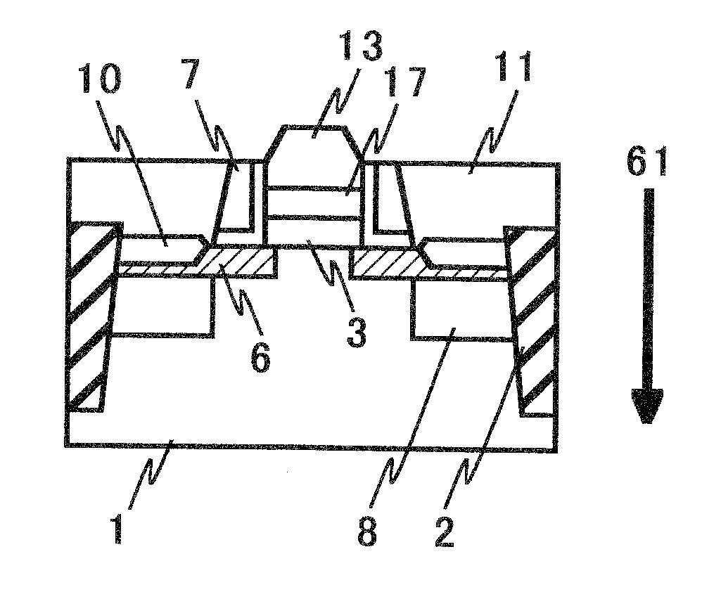
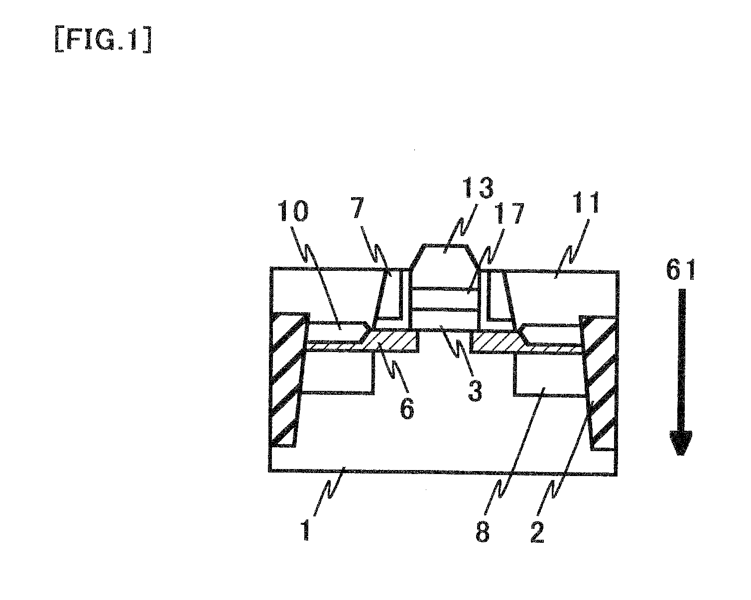
[0107]FIG. 1 is a cross-sectional view illustrating a structure of an NMOSFET in accordance with the first exemplary embodiment of the present invention.

[0108]As illustrated in FIG. 1, the NMOSFET in accordance with the first exemplary embodiment includes a silicon substrate 1, a device separation area 2 formed in the silicon substrate 1, a gate insulating film 3 formed in a p-type region (p-type semiconductor region or p-type well) defined by the device separation area 2, a first gate electrode 13 formed on the gate insulating film 3, a gate sidewall spacer 7 covering a sidewall of the first gate electrode 13 therewith, source / drain regions 8 formed in the silicon substrate 1 to sandwich the p-type region therebetween, extended diffusion layers 6 extending towards the first gate electrode 13 from the source / drain regions 8, silicide layers 10 formed on the extended diffusion layers 6, and an interlayer insulating film 11 formed on the silicide layers 10.

[0109]The first gate electro...

second exemplary embodiment

[0121]A CMOSFET can be fabricated by combining a PMOSFET with the NMOSFET in accordance with the above-mentioned first exemplary embodiment.

[0122]The second exemplary embodiment in accordance with the present invention relates to such a CMOSFET.

[0123]FIGS. 12A to 12C illustrate a CMOSFET in accordance with the second exemplary embodiment of the present invention. FIG. 12A is a plan view of the CMOSFET in accordance with the second exemplary embodiment, FIG. 12B is a cross-sectional view taken along the line A-A′ in FIG. 12A, and FIG. 12C is a combination of a cross-sectional view taken along the line B-B′ in FIG. 12A and a cross-sectional view taken along the line C-C′ in FIG. 12A.

[0124]It should be noted that FIG. 12C is a combination of cross-sectional views of an NMOSFET and a PMOSFET as viewed in different cross-sections, and is not a cross-sectional view obtained when viewed the CMOSFET in a single cross-section. A central broken line in FIG. 12C indicates that an NMOSFET and a...

third exemplary embodiment

[0136]The third exemplary embodiment in accordance with the present invention relates to a method of fabricating the CMOSFET in accordance with the second exemplary embodiment.

[0137]FIGS. 6A to 6H and FIGS. 7A to 7B are cross-sectional views each illustrating respective step in a method of fabricating the CMOSFET, in accordance with the third exemplary embodiment (for simplification, only steps for fabricating an NMOSFET are illustrated in FIGS. 6A to 6H and FIG. 7A).

[0138]First, as illustrated in FIG. 6A, the device separation area 2 was formed at a surface of the silicon substrate 1 through STI (Shallow Trench Isolation) process.

[0139]Then, the electrically insulating layer 3 was formed on a surface of the silicon substrate 1 in a region defined by the device separation area 2. The electrically insulating layer 3 was composed of SiON.

[0140]Then, as illustrated in FIG. 6A, a polysilicon (poly-Si) film 4 was formed on the electrically insulating layer 3 by the thickness of 80 nm.

[01...


PUM


Abstract

The present invention provides an NMOSFET including a semiconductor substrate, a gate insulating film formed on the semiconductor substrate, and a first gate electrode formed on the gate insulating film. The first gate electrode is composed of silicide of a metal M, and at least one element selected as an impurity from a group consisting of sulfur (S), fluorine (F) and chlorine (Cl). The impurity exists as an impurity layer at a surface of the first gate electrode at which the first gate electrode makes contact with the gate insulating film.

Description

BACKGROUND OF THE INVENTION[0001]1. Field of the Invention[0002]The present invention relates to a NMOSFET including a full silicide gate electrode containing impurity therein, a method of fabricating the same, a CMOSFET, and a method of fabricating the same. The present invention relates more particularly to enhancement in performance and reliability of a NMOSFET (N Metal Oxide Semiconductor Field Effect Transistor)[0003]2. Description of the Related Art[0004]In recent development of MOS (Metal Oxide Semiconductor) in which a transistor is fabricated smaller and smaller in size, there is caused a problem that a drive current is deteriorated due to depletion of a polysilicon (poly-Si) electrode.[0005]Thus, some attempts have been made for avoiding deterioration of a driver current by preventing depletion of an electrode by virtue of a metal gate electrode.[0006]In such attempts, a metal gate electrode is composed of pure metal, metal nitride or silicide. Even if a metal gate electro...

Claims


Application Information

Patent Timeline
IPC IPC(8): H01L29/78H01L21/336H01L21/8238
CPCH01L21/28097H01L21/823835H01L21/823842H01L29/7843H01L29/4975H01L29/518H01L21/823871
Inventor MANABE, KENZOIKARASHI, NOBUYUKI
Owner RENESAS ELECTRONICS CORP
Why Eureka
Try Eureka