Semiconductor device for radiation detection
- Summary
- Abstract
- Description
- Claims
- Application Information
AI Technical Summary
Benefits of technology
Problems solved by technology
Method used
Image
Examples
first embodiment
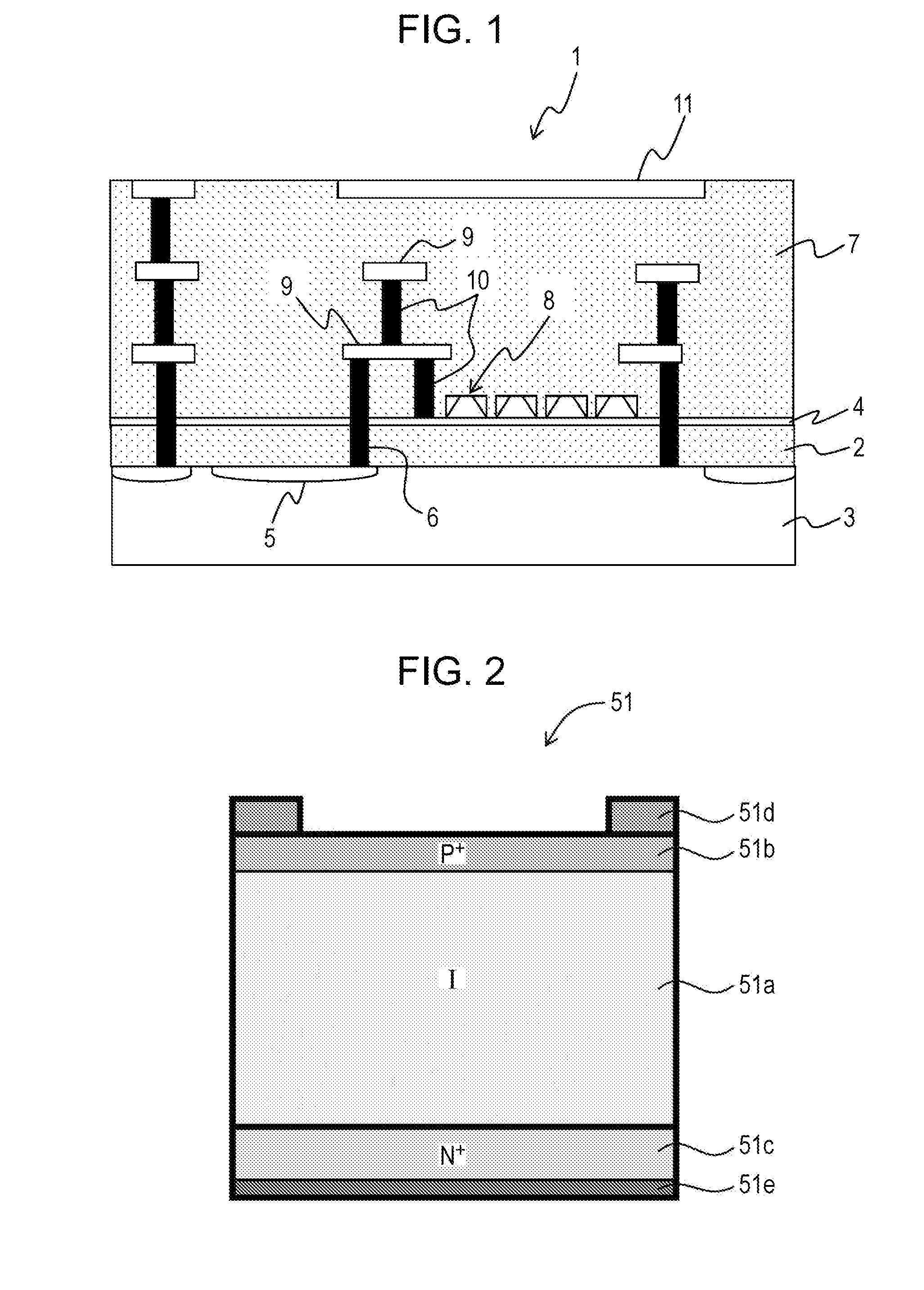
[0104]FIG. 1 is a sectional view illustrating an example of a semiconductor device 1 for radiation detection, according to the first embodiment of the present invention, which has the SOI structure.
[0105]In FIG. 1, the semiconductor device 1 for radiation detection, according to the first embodiment, which has the SOI structure includes an insulator layer 2, a single-crystal silicon layer 3 (or a silicon substrate) which serves as a first semiconductor layer (or a semiconductor substrate) and is disposed on a lower surface of the insulator layer 2, and a single-crystal silicon layer 4 which serves as a second semiconductor layer and is disposed on an upper surface of the insulator layer 2, as the SOI structure.
[0106]In the thick single-crystal silicon layer 3 of the SOI structure, a radiation detection element 5 such as a photodiode and an avalanche photodiode is formed. On the thin single-crystal silicon layer 4 of the SOI structure, a read circuit 8 which reads a signal charge whi...
second embodiment
[0156]In this second embodiment, with the above-described first embodiment, such configuration will be described that a substrate bias potential is self-generated from a source potential via a diffusion resistance layer 46 in a case where the source potential is higher than the substrate bias potential and a source potential is self-generated from a substrate bias potential via the diffusion resistance layer 46 in a case where the source potential is lower than the substrate bias potential.
[0157]FIG. 6 is a sectional view illustrating a MOS transistor element which is formed on the single-crystal silicon layer 4, which is provided on the insulator layer 2, and constitutes the read circuit 8 of a semiconductor device 1F for radiation detection which has the SOI structure and the peripheral portion of the MOS transistor element, according to the second embodiment of the present invention. FIG. 7 is a plan view illustrating an example of the layout configuration of FIG. 6. Here, in FIG...
third embodiment
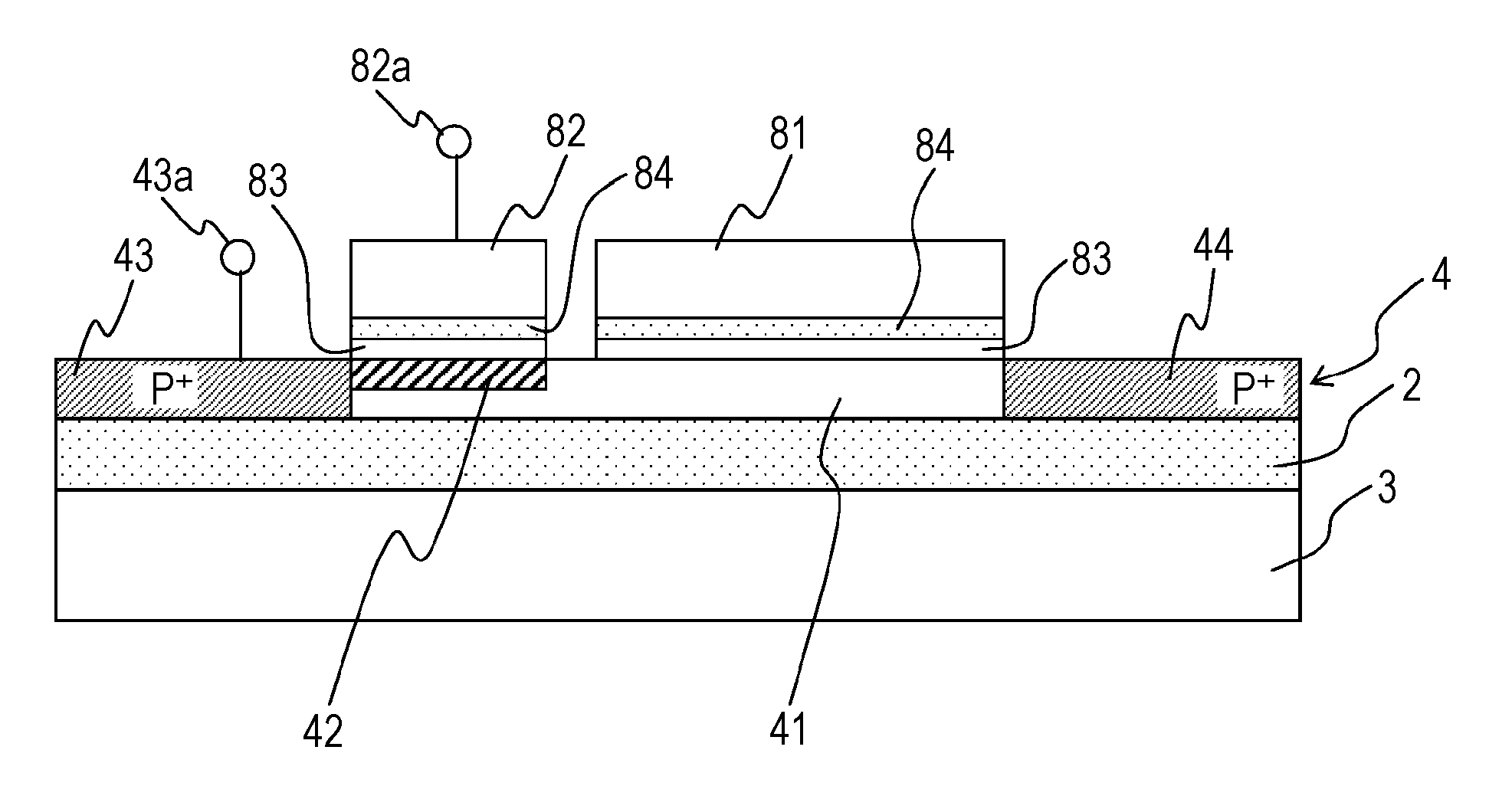
[0162]In the above-described first embodiment, the case where the insulator layer which is disposed to be opposed to the channel region 41 in the MOS transistor is formed to have the laminated structure composed of the silicon nitride film 83 and the silicon oxide film 84 is described. In the above-described second embodiment, with the laminated structure of the above-described first embodiment or instead of this laminated structure, the configuration in which the back gate electrode 48 of the single-crystal silicon layer 4 is connected with the contact electrode 43b of the source region 43 via the diffusion resistance layer 46 and the switch means 47 is described. In a third embodiment, with the laminated structure of the above-mentioned first and second embodiments or instead of this laminated structure, a case where a ferroelectric film having a dielectric polarization characteristic is disposed to be opposed to a channel region of a MOS transistor is described. In this case, the...
PUM
 Abstract
Description
Claims
Application Information


