Insulated-gate semiconductor device and approach involving junction-induced intermediate region

Inactive Publication Date: 2006-06-01
THE BOARD OF TRUSTEES OF THE LELAND STANFORD JUNIOR UNIV
View PDF21 Cites 45 Cited by
  • Summary
  • Abstract
  • Description
  • Claims
  • Application Information

AI Technical Summary

Benefits of technology

[0014] According to a more particular example embodiment, a memory device includes an impact-ionization type device having a subthreshold slope significantly lower than kT / q leading up to a threshold voltage required for current switching. The device may be implemented with a wide variety of circuit structures, for example, such as for storing data at a node coupled for maintaining a charge. The data storage is controlled as a function of a threshold voltage applied for controlling the conductance state of the device. With this approach, the threshold voltage required for effecting current switching can be reduced without necessarily significantly affecting current flow, relative to the threshold voltage-current relationship for conventional transistors with higher subthreshold slopes. Furthermore, this reduction in threshold voltage is achieved while maintaining acceptable levels of leakage during an off (current-blocking) state, effecting rapid switching and data transfer with low power consumption.

Problems solved by technology

Recent technological advances in the semiconductor industry have permitted dramatic increases in circuit density and complexity, and commensurate decreases in power consumption and package sizes for integrated circuit devices.
These and other demands have led to increased pressure to manufacture a large number of semiconductor devices at an efficient pace while increasing the complexity and improving the reliability of the devices.
For instance, higher voltage generally relates to higher dynamic power dissipation per device and correspondingly higher overall dynamic power dissipation of the chip in which the device is employed.
In addition, higher voltage also generally relates to larger electric fields within the device, which can sometimes adversely affect the reliability of the operation of the device.
However, this reduction in supply voltage affects the ability of the device to maintain current in its ON-state; namely, the threshold voltage for maintaining current must still be met.
Scaling of the threshold voltage, however, is challenging for a variety of reasons.
This means that decreasing threshold voltages lead to increasing leakage currents through these devices because the inverse subthreshold slope (the slope of a plot of the amount of current passed in the device versus gate voltage) is limited to a thermodynamic value of kT / q or 60 mV / decade at about room temperature.
These and other considerations have presented challenges to the implementation and advancement of switching circuitry, and in particular for low-power, highly-reliable circuitry.
In addition, these approaches facilitate the integration of an increasingly larger number of transistors at increasing clock frequencies at a relatively modest increase in overall dynamic power dissipation of a circuit employing these devices.

Method used


Image

  • Insulated-gate semiconductor device and approach involving junction-induced intermediate region
  • Insulated-gate semiconductor device and approach involving junction-induced intermediate region
  • Insulated-gate semiconductor device and approach involving junction-induced intermediate region

Examples


Embodiment Construction

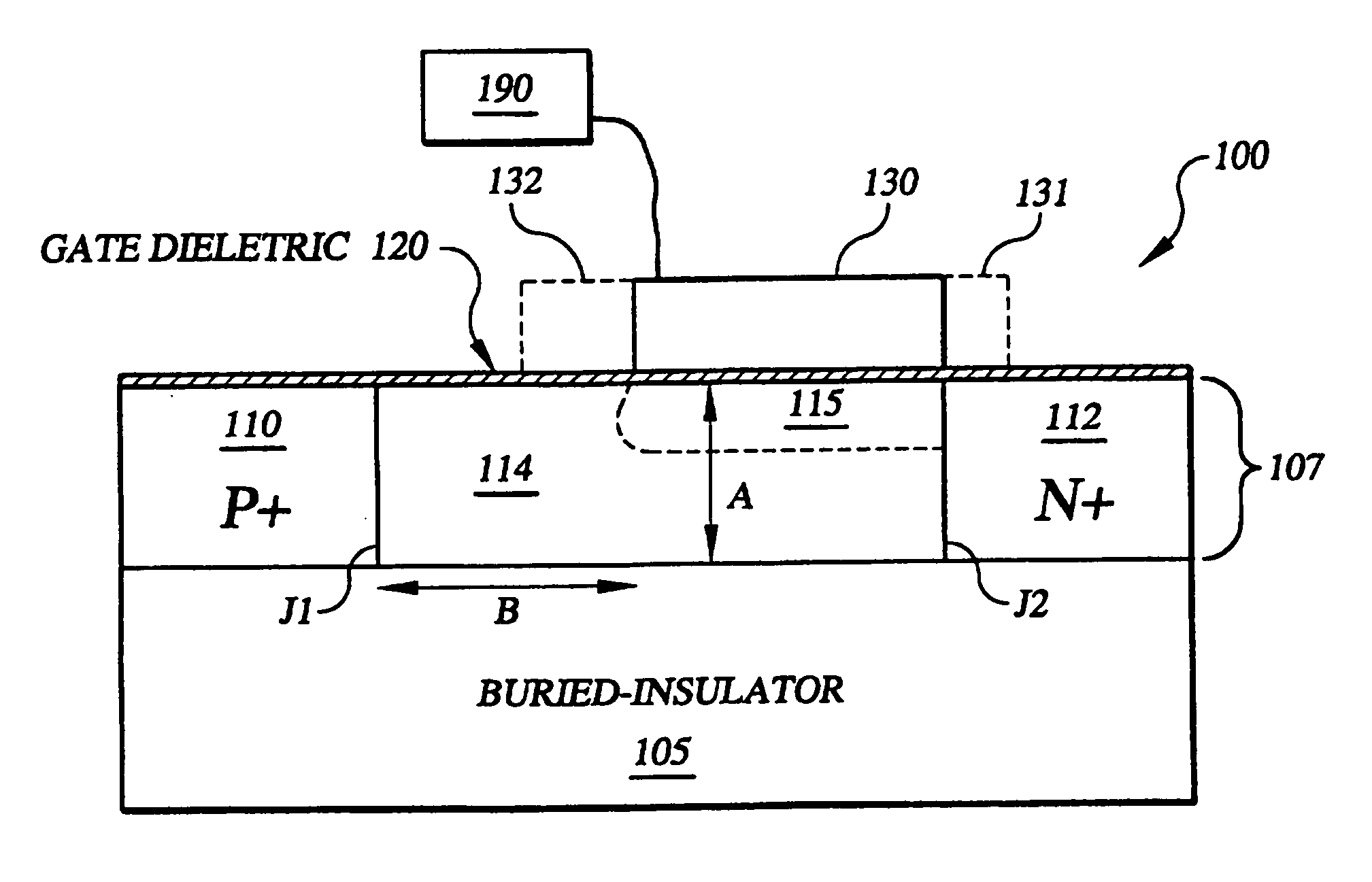
[0035] The present invention is believed to be applicable to a variety of different types of semiconductor devices, and the invention has been found to be particularly suited for devices in the deep-sub-micron regime, such as MOS devices and other field-effectable structures adapted to respond to a voltage at its capacitively-coupled gate by accumulating carriers under the gate and forming an accumulation surface channel. While the present invention is not necessarily limited to such applications, various aspects of the invention may be appreciated through a discussion of various examples using this context.

[0036] According to an example embodiment of the present invention, an insulated-gate device includes an intermediate region defined by metallurgical junctions (as described above) and between two oppositely-doped regions. The oppositely-doped regions have a relatively high dopant concentration (e.g., one being N+ and the other P+), while the intermediate region is relatively ne...


PUM


Abstract

Semiconductor device performance is improved via an insulated-gate PIN-type structure that is adapted to abruptly switch between conductance states by modulating an electric field in the intermediate (I) region. According to an example embodiment of the present invention, an insulated gate-type structure includes a body with first and second end regions and an intermediate region coupled therebetween, the intermediate region having a length defined by junctions at the first and second regions. The first and second end regions have opposite polarizations and the intermediate region has a polarization that is neutral relative to the polarizations of the first and second end regions. The insulated gate-type structure also includes a gate that is coupled to the intermediate region and adapted, with the intermediate region, to apply an electric field nearer one of the two junctions. With the body reverse biased, the electric field can be modulated to switch the structure between a stable state and a current-conducting state in which an avalanche breakdown occurs in the intermediate region.

Description

FIELD OF THE INVENTION [0001] The present invention relates generally to semiconductor devices and more specifically to semiconductor devices having a reverse-biased multi-region body having oppositely doped end regions on either side of an intermediate region and having a gate structure used to facilitate current switching. BACKGROUND OF THE INVENTION [0002] Recent technological advances in the semiconductor industry have permitted dramatic increases in circuit density and complexity, and commensurate decreases in power consumption and package sizes for integrated circuit devices. Single-chip microprocessors now include many millions of transistors (e.g. bipolar junction transistors (BJT) and metal oxide semiconductor (MOS) devices) operating at speeds of hundreds of millions of instructions per second to be packaged in relatively small, air-cooled semiconductor device packages. A by product of these technological advances has been an increased demand for semiconductor-based produc...

Claims


Application Information

Patent Timeline
IPC IPC(8): H01L29/94G11C11/404G11C11/405H01L27/105H01L29/739
CPCH01L27/105H01L29/7391H01L29/785G11C11/404G11C11/405H10B99/22
Inventor GOPALAKRISHNAN, KAILASHPLUMMER, JAMES D.
Owner THE BOARD OF TRUSTEES OF THE LELAND STANFORD JUNIOR UNIV
Why Eureka
Try Eureka