Chip scale package and method of fabricating the same
Inactive Publication Date: 2010-09-02
ADVANCED SEMICON ENG INC
View PDF6 Cites 10 Cited by
Summary
Abstract
Description
Claims
Application Information
AI Technical Summary
This helps you quickly interpret patents by identifying the three key elements:
Problems solved by technology
Method used
Benefits of technology
Benefits of technology
[0009]The invention is directed to a chip scale package (CSP) structure and a method of manufacturing the same. The heat dissipation efficiency of the package structure is increased, the bond line thickness (BLT) of the package structure is controlled, and the package products being fabricated have the advantages of high heat dissipation efficiency and low thickness.
Problems solved by technology
Thus, the lead-frame packaging no longer capable of satisfying the market needs.
Of the chip scale package (CSP) structures currently available including the wire bonding and the flip chip CSP package structure alike, a complicated manufacturing process is required for disposing the heat spreader on the CSP structure to increase the heat-dissipation effect.
Thus, the heat-dissipation effect is increased at the cost of an increased manufacturing cost.
Method used
Image
Click on the blue label to locate the original text in one second.
Reading with bidirectional positioning of images and text.
Examples
first embodiment
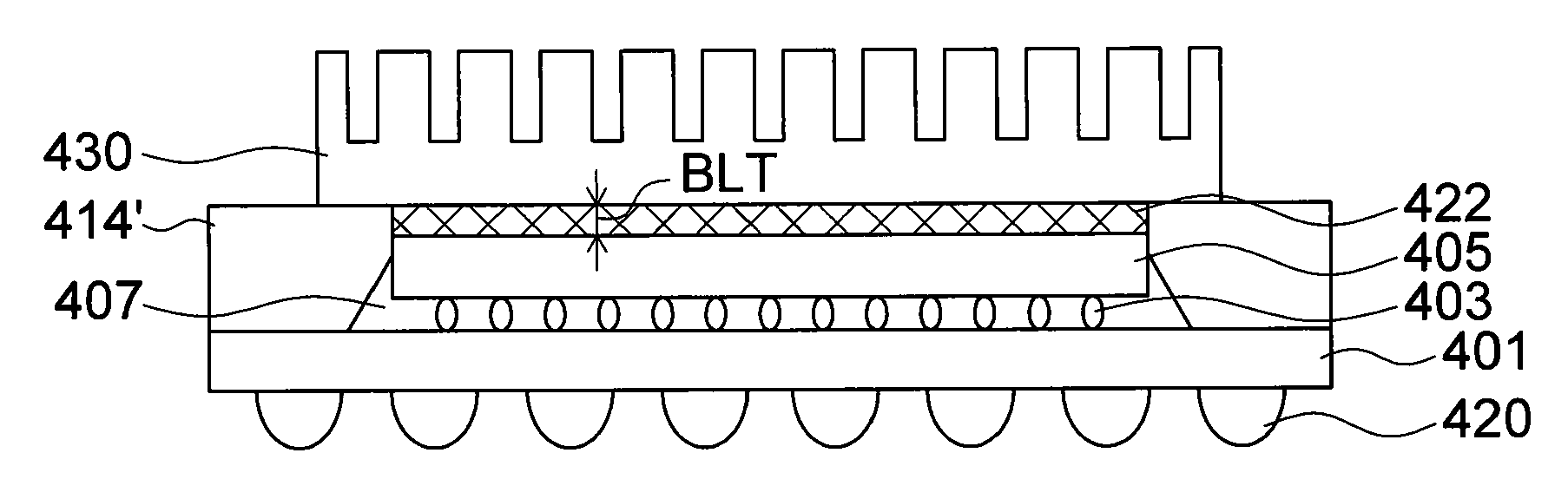
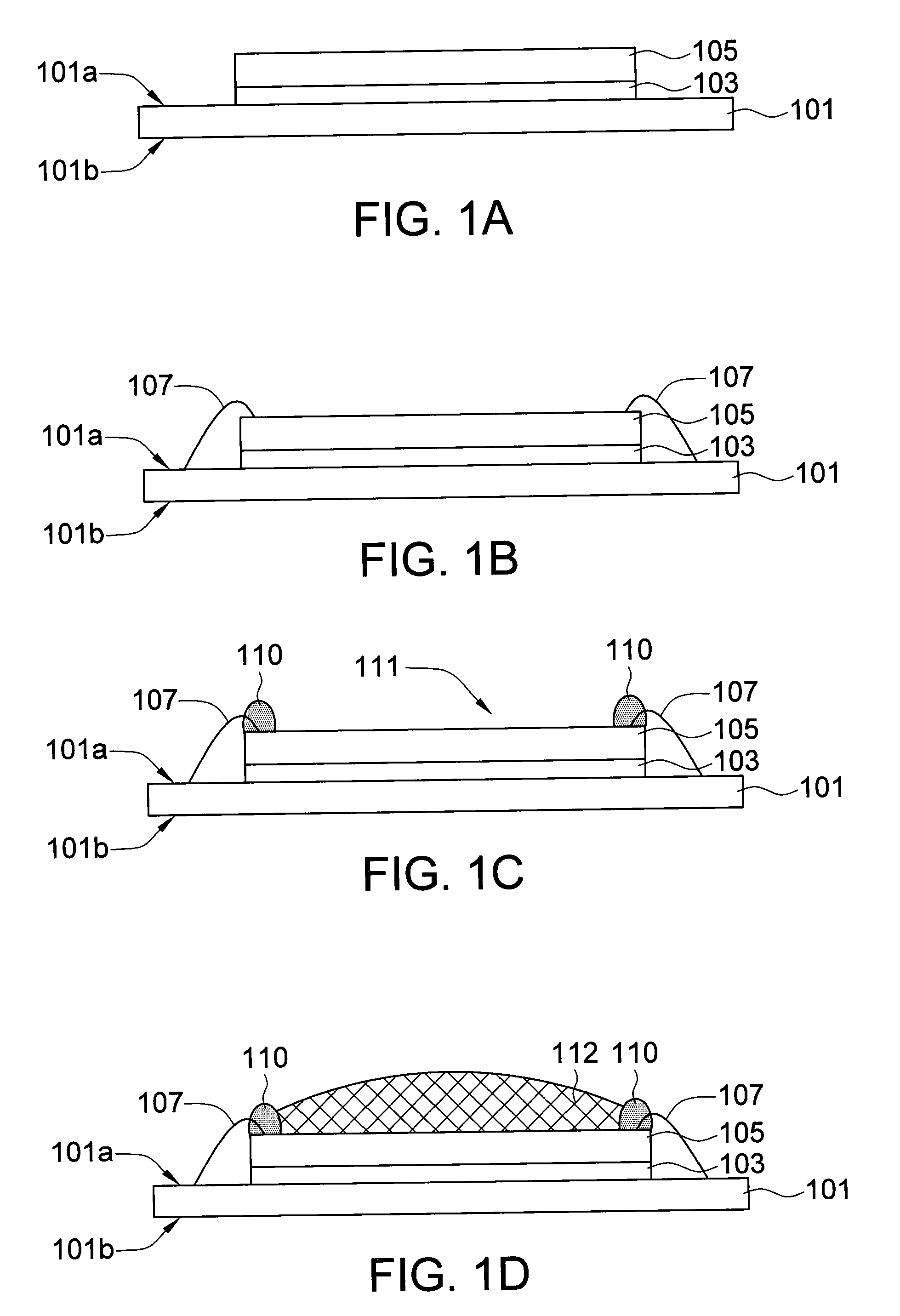
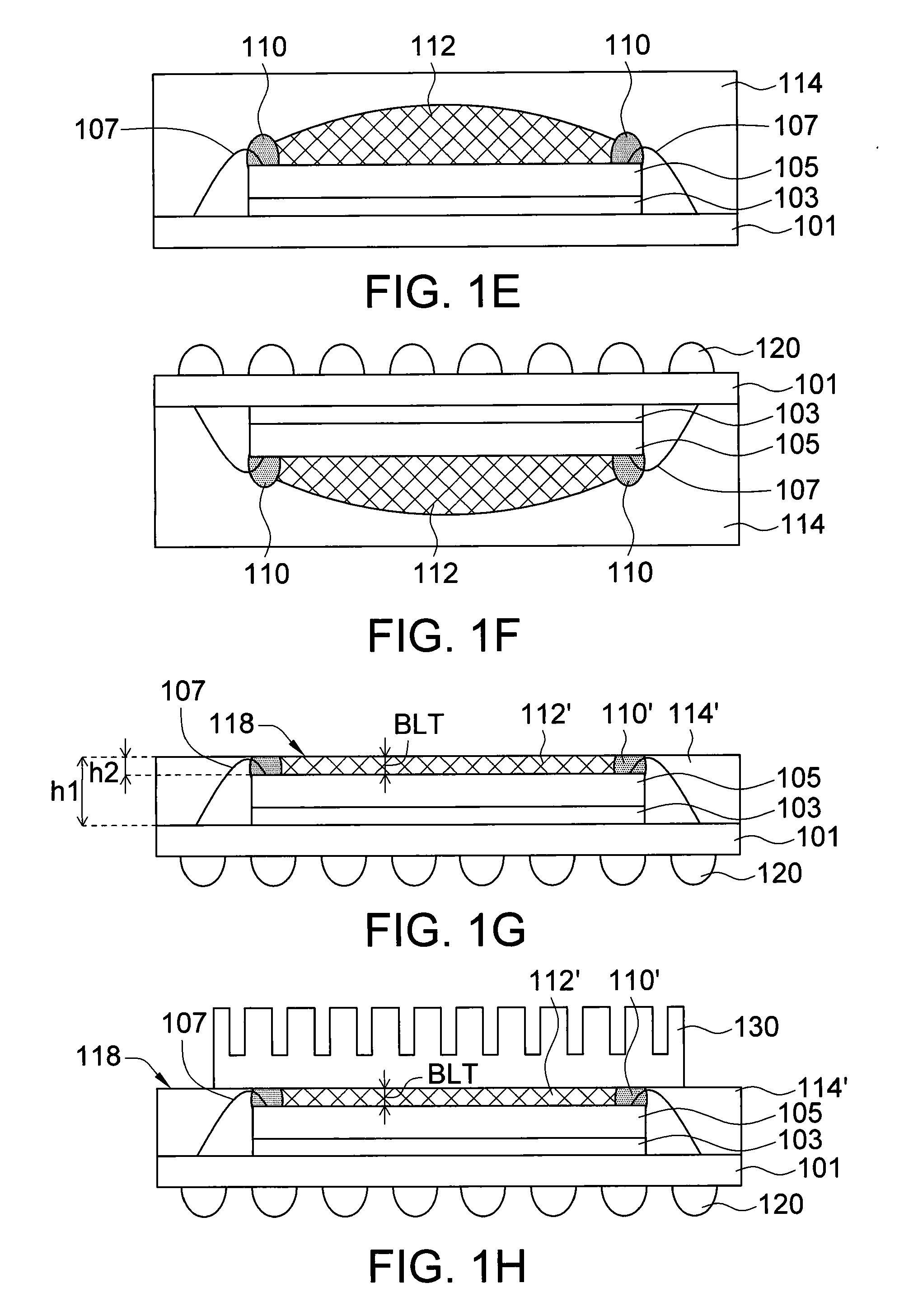
[0023]Referring to FIG. 1A˜FIG. 1H, a method of fabricating a CSP structure according to a first embodiment of the invention is shown. First, a substrate 101 is provided, and an adhesive 103 is used for fixing the rear surface of a chip 105 on the front surface 101a of the substrate 101, as shown in FIG. 1A. Next, a number of wires 107 are used for electrically connecting the front surface (the electrode surface) of the chip 105 with the substrate 101 by way of wire bonding, as shown in FIG. 1B.
[0024]Then, a dam-like non-conductive paste 110 is formed on the front surface of the chip 105, wherein the non-conductive paste 110 further covers the wires 107, as shown in FIG. 1C. The non-conductive paste 110 defines a receiving area 111 on the front surface of the chip 105. The non-conductive paste is made from a non-electrically conductive material such as epoxy or the like.
[0025]Afterwards, a thermal conductive paste 112 is filled within the receiving area 111. Then, a heating step is ...
second embodiment
[0031]Referring to FIG. 2A˜FIG. 2H, a method of fabricating a CSP structure according to a second embodiment of the invention is shown. In the second embodiment, the chip is bonded by way of flip-chip bonding.
[0032]First, a substrate 201 is provided, and conductive bumps such as a tin-lead protrusion 203 is used for flip-bonding the chip 205 on the front surface 201a of the substrate 201 by way of soldering with the front surface (the electrode surface) of the chip 205 facing downward, as shown in FIG. 2A. Compared with the way of wire-bonding, the advantage of using the tin-lead protrusion is that the flip chip package largely increases the density of the input / output (I / O) contacts of the chip. Next, an underfill 207 can be selected and filled between the chip 205 and the substrate 201 as shown in FIG. 2B.
[0033]Then, as shown in FIG. 2C, a thermal conductive paste 212 is disposed on the surface (that is, the rear surface 205b) of the chip 205, and then the thermal conductive paste...
third embodiment
[0037]Referring to FIG. 3A˜FIG. 3I, a method of fabricating a CSP structure according to a third embodiment of the invention is shown. In the third embodiment, the chip is bonded by way of flip-chip bonding. The present embodiment is very similar to the second embodiment except that in the present embodiment, a dam-like non-conductive paste is formed before the thermal conductive paste is used to avoid the thermal conductive paste overflowing. The steps of the third embodiment are disclosed below.
[0038]First, a substrate 301 is provided, and conductive bumps such as a tin-lead protrusion 303 is used for flip-bonding the front surface of (the electrode surface) of the chip 305 on the front surface 301a of the substrate 301, as shown in FIG. 3A. It is noted that the chip 305 could be electrically connected with the substrate 301 other types of conductive materials, and tin-lead is merely exemplified as one material of conductive bumps. Next, an underfill 307 is selected and filed betw...
PUM
Abstract
A chip scale package (CSP) package and method of fabricating the same are provided. The fabricating method includes the following steps. First, a substrate is provided. Next, a chip is disposed on the front surface of the substrate and electrically connected to the substrate. Then, a thermal conductive paste is formed on the surface of the chip. Afterwards, a molding compound for enclosing the chip is formed. Lastly, a milling process is applied to the molding compound so that the height of the molding compound is aligned with that of the thermal conductive paste. The chip can be disposed on the substrate by way of wire bonding or flip-chip bonding. The thermal conductive paste is disposed on the surface of the chip either before or after the milling process is completed.
Description
[0001]This application claims the benefit of Taiwan application Serial No. 98106567, filed Feb. 27, 2009, the subject matter of which is incorporated herein by reference.BACKGROUND OF THE INVENTION[0002]1. Field of the Invention[0003]The invention relates in general to a package structure and a method of manufacturing the same, and more particularly to a chip scale package (CSP) structure with high heat dissipation efficiency and a method of manufacturing the same.[0004]2. Description of the Related Art[0005]Along with the advance in electronic technology, high-tech electronic products are available in the market one after another. The main purpose of the package industry is to support the research and development of electronic products and assure (1) the speed of semi-conductor packages continues to increase, (2) the functions of the semi-conductor packages are fully availed, and (3) the electronic products incorporating semi-conductor package posses the advantages of slimness, lig...
Claims
Application Information
Patent Timeline
Application Date:The date an application was filed.
Publication Date:The date a patent or application was officially published.
First Publication Date:The earliest publication date of a patent with the same application number.
Issue Date:Publication date of the patent grant document.
PCT Entry Date:The Entry date of PCT National Phase.
Estimated Expiry Date:The statutory expiry date of a patent right according to the Patent Law, and it is the longest term of protection that the patent right can achieve without the termination of the patent right due to other reasons(Term extension factor has been taken into account ).
Invalid Date:Actual expiry date is based on effective date or publication date of legal transaction data of invalid patent.

