
Ceramic composite multilayer substrate, method for manufacturing ceramic composite multilayer substrate and electronic component

Active Publication Date: 2010-09-09
MURATA MFG CO LTD
View PDF2 Cites 24 Cited by
  • Summary
  • Abstract
  • Description
  • Claims
  • Application Information

AI Technical Summary

Benefits of technology

[0012]In order to solve the above-described problems, preferred embodiments of the present invention provide a high-reliability ceramic composite multilayer substrate that has excellent flatness and few remaining pores, can be produced at a low cost while simplifying the manufacturing process, and can eliminate layer separation or separation from a mother board, for example, a method for manufacturing the same, and electronic components.
[0013]A ceramic composite multilayer substrate according to a preferred embodiment of the present invention includes a laminate including a first ceramic layer and a second ceramic layer that is disposed so as to contact the first ceramic layer and to suppress firing shrinkage in the plane direction of the first ceramic layer, in which the laminate includes a resin / ceramic composite layer in which porous ceramic is impregnated with a resin provided on at least one principal surface of the laminate.
[0033]An electronic component according to a preferred embodiment of the present invention includes a laminate including a first ceramic layer and a second ceramic layer that is disposed so as to contact the first ceramic layer and suppresses firing shrinkage in the plane direction of the first ceramic layer, in which a mounting device is placed on one principal surface of a ceramic composite multilayer substrate including a resin / ceramic composite layer in which porous ceramic is impregnated with a resin on at least one principal surface of the laminate.
[0034]Preferred embodiments of the present invention can provide a high-reliability ceramic composite multilayer substrate that has excellent flatness and few remaining pores, can be produced at a low cost while simplifying the manufacturing process, and can eliminate layer separation or separation from a mother board, for example, a method for manufacturing the same, and electronic components.

Problems solved by technology

In this composite multilayer substrate, a gradient structure is given to the thermal expansion coefficient because there is a possibility that layer separation or cracks may occur due to thermal shock at an interface having a large thermal expansion coefficient difference when the thermal expansion coefficient of a composite resin material layer is adjusted to the thermal expansion coefficient of either one of the ceramic substrate or a printed-circuit board.
However, when the ceramic substrate is warped before the formation of the resin layer or the ceramic substrate is warped due to the formation of the resin layer, cracks are likely to occur.
Due to the reduction in the layer thickness, the ceramic substrate is likely to be warped or cracks are likely to occur during resin curing.
In such a case, the generation of cracks is difficult to suppress.
Furthermore, since the resin layer is formed more than once, position shift or the like occurs between the resin layers while laminating the resin layers, reducing the lamination accuracy so as to deteriorate the shape of the resin layers deteriorates, and thus the composite multilayer substrate is likely to deform.
According to the method including forming the resin layer more than once, it has been difficult to make the thickness of the ceramic substrate uniform after the formation of the substrate is completed and moreover it has been difficult to smooth the resin layer on the substrate surface.
Accordingly, the same process is repeatedly performed when forming the resin layer, which has caused problems in that the manufacturing method has become complicated and structural defects have been likely to occur when forming a wiring structure.

Method used


Image

  • Ceramic composite multilayer substrate, method for manufacturing ceramic composite multilayer substrate and electronic component
  • Ceramic composite multilayer substrate, method for manufacturing ceramic composite multilayer substrate and electronic component
  • Ceramic composite multilayer substrate, method for manufacturing ceramic composite multilayer substrate and electronic component

Examples


first preferred embodiment

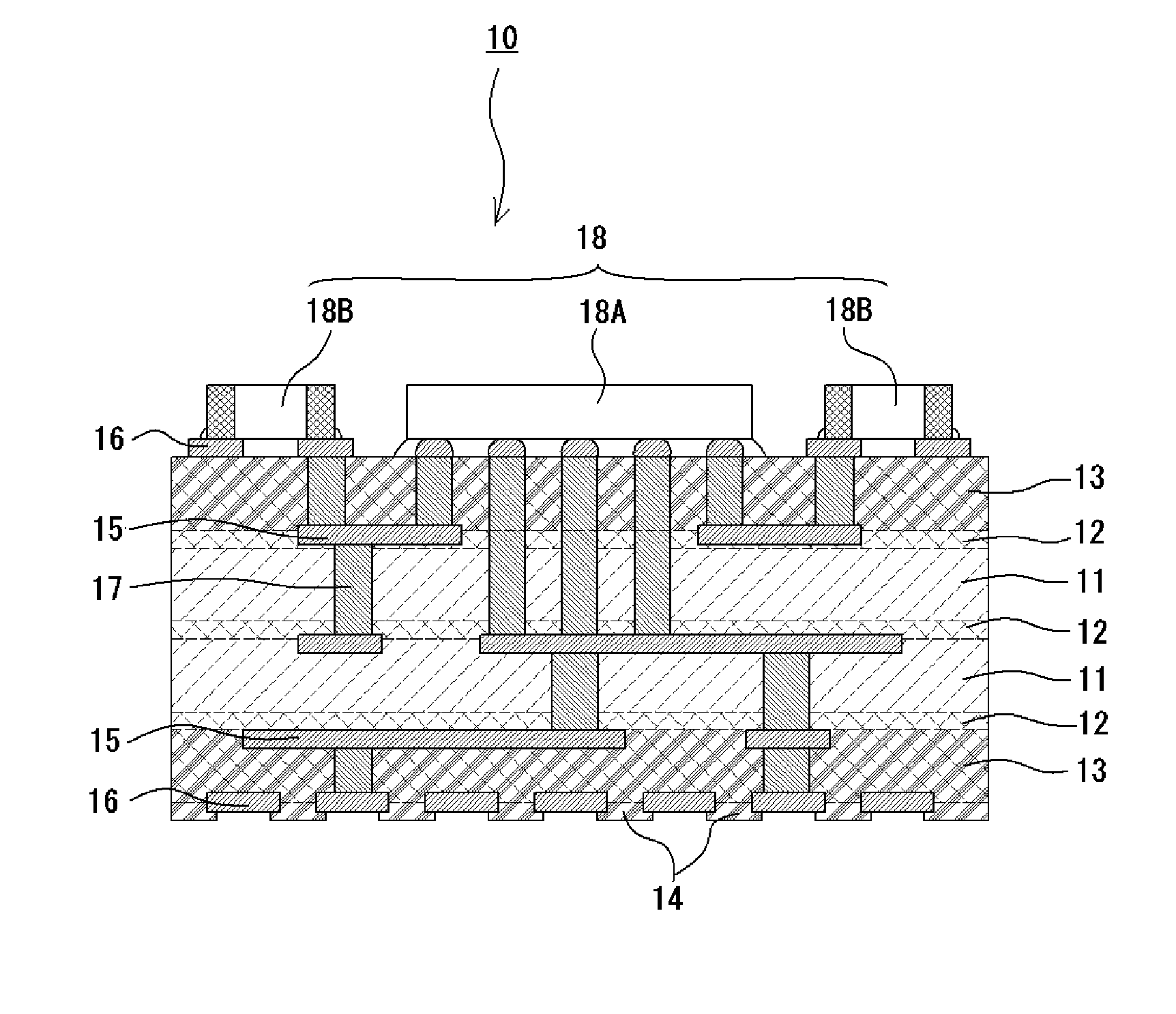
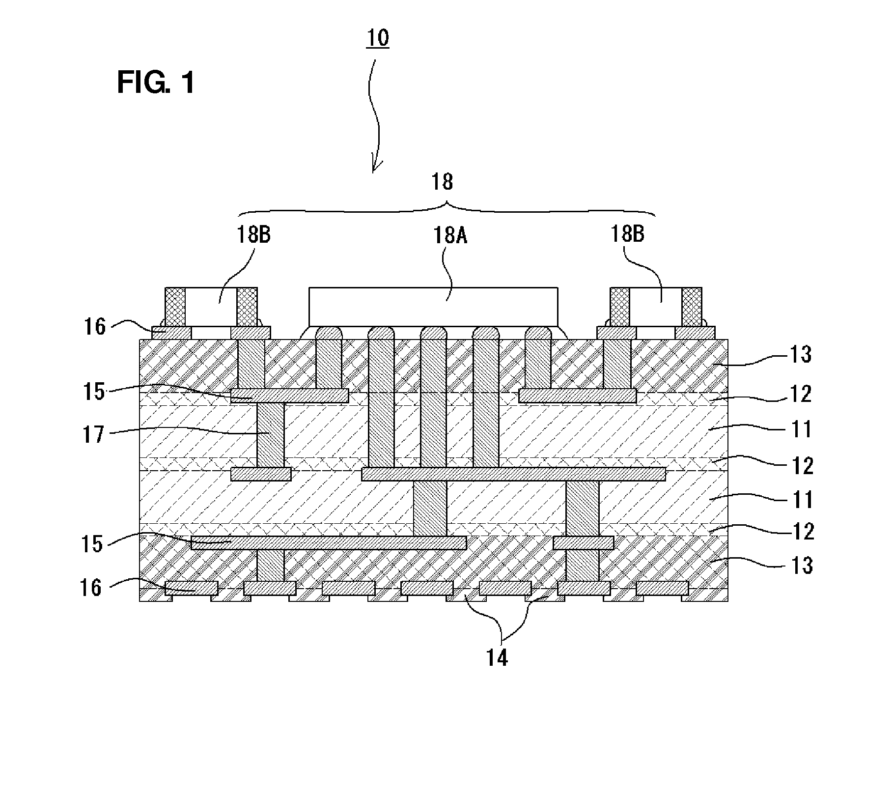
[0048]A ceramic composite multilayer substrate 10 of this preferred embodiment preferably includes, as shown in FIG. 1, for example, a first ceramic layer 11, a second ceramic layer 12 that is laminated so as to contact one principal surface (upper surface) of the first ceramic layer and functions as an internal constraining layer, and a resin / ceramic composite layer 13 that is laminated so as to contact the principal surface (upper surface) of the second ceramic layer 12 and is impregnated with a resin. On the other principal surface (undersurface) of the first ceramic layer 11, the second ceramic layer 12, the first ceramic layer 11, the second ceramic layer 12, and the resin / ceramic composite layer 13 are laminated toward the bottom in this order. When the first and second ceramic layers 11 and 12 and the resin / ceramic composite layer 13 are considered to be one composite laminate, the ceramic composite multilayer substrate 10 has another composite laminate laminated on the under...

second preferred embodiment

[0075]As shown in FIG. 7, a ceramic composite multilayer substrate 10A of this preferred embodiment is structured similarly as in the first preferred embodiment, except that the ceramic composite multilayer substrate 10A is not provided with the second ceramic layer 12 disposed between the first ceramic layer and the resin / ceramic composite layer 13 at the upper side and the resin / ceramic composite layer 13 at the lower side in the ceramic composite multilayer substrate 10 of the first preferred embodiment. Accordingly, the same reference numbers are used also in this preferred embodiment for components which are the same as or equivalent to those in the first preferred embodiment.

[0076]In order to obtain a flat substrate after firing, the porous ceramic layers 13A acting as a resin-impregnated layer are preferably disposed with the same thickness on both sides of the ceramic substrate. However, the structure is not limited to the above depending on the structure of the ceramic comp...

third preferred embodiment

[0077]As shown in FIG. 8, a ceramic composite multilayer substrate 10B of this preferred embodiment is structured similarly as in the first preferred embodiment, except that the second ceramic layers 12 disposed between the first ceramic layers 11 and the resin / ceramic composite layers 13 disposed at the upper and lower sides, respectively, in the ceramic composite multilayer substrates 10 of the first preferred embodiment are omitted. Accordingly, the same reference numbers are used also in this preferred embodiment for components that are the same as or equivalent to those in the first preferred embodiment.

[0078]In order to obtain a high-precision ceramic composite multilayer substrate 10 in which firing shrinkage in the in-plane direction is suppressed as in the ceramic composite multilayer substrate 10 of the first preferred embodiment, it is preferable to dispose the second ceramic layer 12 having a required thickness in the lamination direction for every at least 40 μm, for ex...


PUM

PropertyMeasurementUnit
Lengthaaaaaaaaaa
Lengthaaaaaaaaaa
Lengthaaaaaaaaaa

Abstract

A high-reliability ceramic composite multilayer substrate that has excellent flatness and few remaining pores, can be produced at a low cost while simplifying the manufacturing process, and can eliminate layer separation or separation from a mother board. The ceramic composite multilayer substrate includes a laminate containing a first ceramic layer and a second ceramic layer that is disposed so as to contact the first ceramic layer and suppresses firing shrinkage in the plane direction of the first ceramic layer. The laminate includes a resin / ceramic composite layer in which porous ceramic is impregnated with a resin formed on at least one principal surface of the laminate.

Description

BACKGROUND OF THE INVENTION[0001]1. Field of the Invention[0002]The present invention relates to a ceramic composite multilayer substrate, a method for manufacturing the same, and electronic components.[0003]2. Description of the Related Art[0004]As techniques relating to ceramic multilayer substrates, the techniques described in Japanese Unexamined Patent Application Publication No. 05-136572, Japanese Unexamined Patent Application Publication No. 2005-210036 and Japanese Unexamined Patent Application Publication No. 2005-223226 are known, for example. Japanese Unexamined Patent Application Publication No. 05-136572 describes a method for manufacturing a multilayer ceramic substrate, and Japanese Unexamined Patent Application Publication No. 2005-210036 and Japanese Unexamined Patent Application Publication No. 2005-223226 each describes a composite multilayer substrate.[0005]The method for manufacturing a multilayer ceramic substrate described in Japanese Unexamined Patent Applica...

Claims


Application Information

Patent Timeline
IPC IPC(8): H05K1/00B32B3/26C04B35/84B32B18/00C04B37/00
CPCH05K1/0306Y10T29/49163H05K3/4688H05K2201/0116H05K2203/1147B32B9/005B32B9/04B32B9/045B32B18/00B32B3/08C04B35/111B32B2250/40B32B2260/02B32B2260/046C04B2235/365C04B2235/5436C04B2235/5445C04B2235/5472C04B2235/6025C04B2237/343C04B2237/345C04B2237/346C04B2237/348C04B2237/62C04B2237/66C04B2237/704C04B2237/68H05K3/4629Y10T428/24331H01L2924/19105H01L2924/15192Y10T428/24777H01L2224/16225H01L2224/32225H01L2224/73204H01L2924/00H01L2924/00014H01L2224/16227H01L2924/15313H01L2924/00011Y10T428/249994H01L2224/0401
Inventor NOMIYA, MASATO
Owner MURATA MFG CO LTD
Learn More