Semiconductor device

Active Publication Date: 2010-09-09
DENSO CORP
View PDF15 Cites 12 Cited by
  • Summary
  • Abstract
  • Description
  • Claims
  • Application Information

AI Technical Summary

Benefits of technology

[0025]According to the technique taught in the present specification, a semiconductor device with increased

Problems solved by technology

However, the method of Patent Document 1 cannot be adopted in the IGBT.
If the thickness of the buffer layer i

Method used


Image

  • Semiconductor device
  • Semiconductor device
  • Semiconductor device

Examples


first embodiment

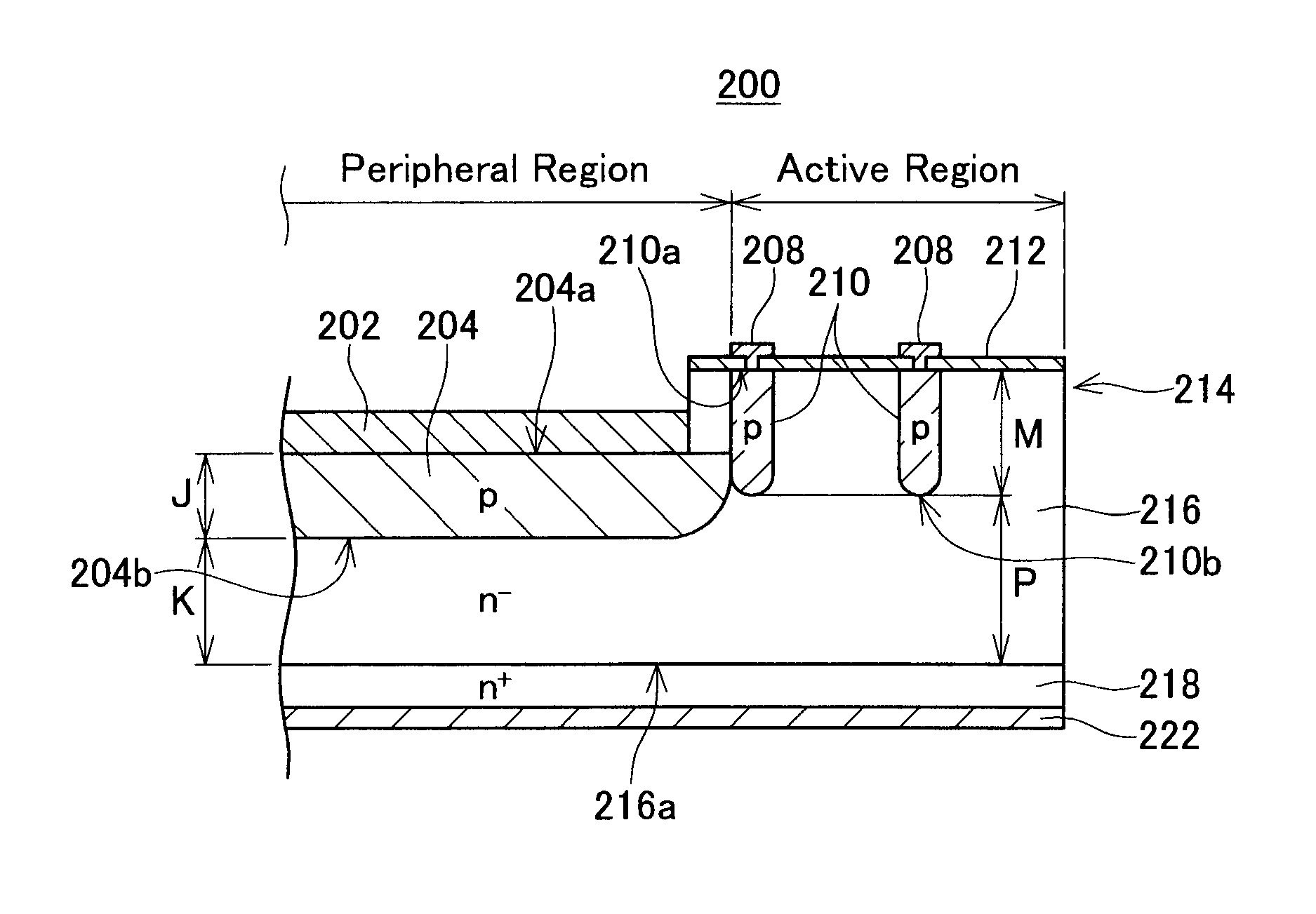
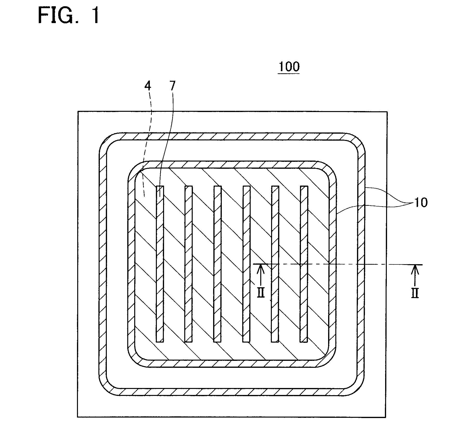
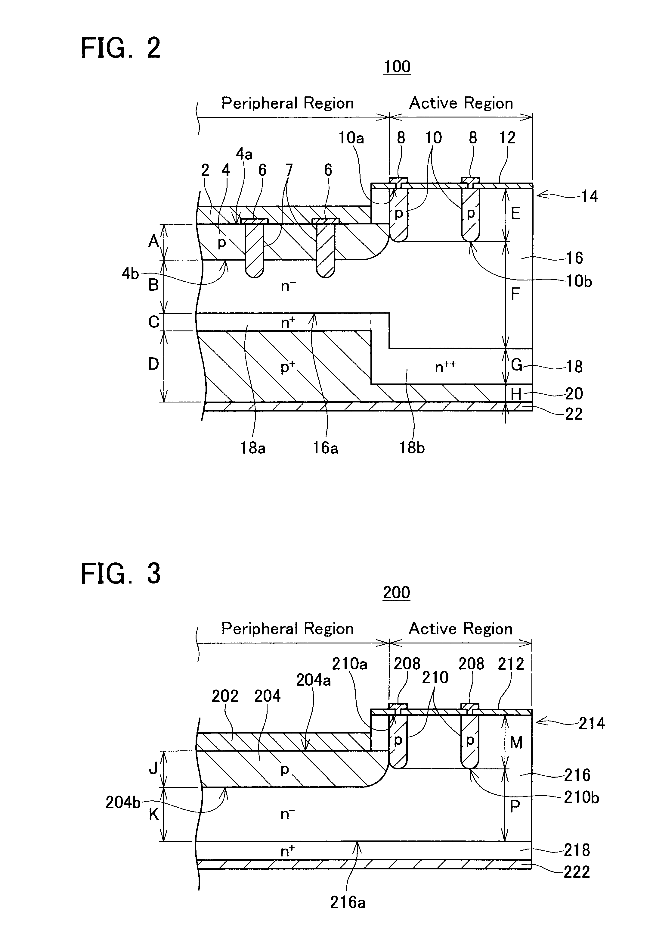
[0029]A semiconductor device of the first embodiment will be explained with reference to FIGS. 1, 2. The semiconductor device of the present embodiment is an example in which the present invention has been applied to an IGBT. FIG. 1 is a schematic plan view of an IGBT 100. FIG. 2 is a schematic cross-sectional view of the IGBT 100 viewed along the line II-II of FIG. 1.

[0030]First, an outline of the configuration of the IGBT 100 will be given. The IGBT 100 is formed on a semiconductor substrate 14. Below, the “semiconductor substrate 14” is termed simply “substrate 14”. A metal collector electrode 22 is formed on a back surface of the substrate 14. A p+-type collector layer 20 (third semiconductor layer) is formed on an upper surface of the collector electrode 22, i.e. on a bottom layer of the substrate 14. An n-type buffer layer 18 (high impurity concentration layer) is formed on the collector layer 20. The concentration of the n-type impurities in the buffer layer 18 will be descri...


PUM


Abstract

To provide a semiconductor device in which dielectric breakdown strength in a peripheral region is increased without increasing on-resistance. An IGBT comprises a body region, guard ring, and collector layer. The body region is formed within an active region in a surface layer of a drift layer. The guard ring is formed within a peripheral region in the surface layer of the drift layer, and surrounds the body region. The collector layer is formed at a back surface side of the drift layer, and is formed across the active region and the peripheral region. A distance F between a back surface of the guard ring and the back surface of the drift layer is greater than a distance between a back surface of the body region and the back surface of the drift layer. A thickness H of the collector layer in the peripheral region is smaller than a thickness D of the collector layer in the active region.

Description

TECHNICAL FIELD[0001]This application claims priority to Japanese Patent Application No. 2007-289536, filed on Nov. 7, 2007, the contents of which are hereby incorporated by reference into the present application. The present invention relates to a semiconductor device whose dielectric breakdown strength (voltage resistance) is increased without increasing its resistance while conducting. For example, the present invention relates to an IGBT with low on-voltage and high dielectric breakdown strength, or a diode with low forward voltage drop and high dielectric breakdown strength. In the present specification, “low resistance while conducting” means that forward voltage drop, on-resistance, or on-voltage is low.BACKGROUND ART[0002]A semiconductor device is known that comprises a semiconductor substrate which, in a plan view, includes an active region in which a semiconductor element is formed and a peripheral region that surrounds the active region. The phrase “a plan view of the sem...

Claims


Application Information

Patent Timeline
IPC IPC(8): H01L29/739H01L29/06
CPCH01L29/0619H01L29/0657H01L29/8611H01L29/404H01L29/7397H01L29/0696H01L2924/10155
Inventor HARA, MASAFUMI
Owner DENSO CORP
Why Eureka
Try Eureka