
Implementing Tamper Resistant Integrated Circuit Chips

a technology of integrated circuit chips and tamper-resistant chips, applied in the field of data processing, can solve the problems of increasing the number of counterfeiting of chip design and processing methods, the inability to adequately protect intellectual property, and the danger of that technology falling into the enemy's hands

Active Publication Date: 2010-09-09
TERRACE LICENSING LLC
View PDF11 Cites 46 Cited by
  • Summary
  • Abstract
  • Description
  • Claims
  • Application Information

AI Technical Summary

Benefits of technology

[0015]Principal aspects of the present invention are to provide a method and tamper resistant circuit for resisting tampering including reverse engineering in a semiconductor chip, and a design structure on which the subject circuit resides. Other important aspects of the present invention are to provide such method, circuit and design structure substantially without negative effect and that overcome many of the disadvantages of prior art arrangements.

Problems solved by technology

Failure to adequately protect intellectual property is very damaging to the semiconductor industry.
In addition, a significant military concern associated with placing high technology on the battlefield is the risk of that technology falling into the enemy's hands.
There are an increasing number of instances of the counterfeiting of chip design and processing methods.
One form of counterfeiting is the unauthorized direct copying of the integrated circuit (IC), and reproduction of its layout design and topography or mask work, the fabrication of an IC based on this mask work and the sale of the resulting chips under a different company's name.
Another form of counterfeiting involves illegally reverse engineering a competitor's IC and stealing the design material and process recipes.
Often destructive methods require de-packaging, and sometimes at least partially dissecting the IC, making it impossible to use the IC afterwards.
Further, these prior art methods typically involve significant manual intervention by skilled personnel.
Therefore, the methods are very expensive and time consuming.
In addition, some types of information about circuits, such as the contents of non-volatile semiconductor memories cannot be obtained by using this method.
This method may be ineffective because the PICA technique can include detecting optical emission from the front side as well as backside of the chip.

Method used


Image

  • Implementing Tamper Resistant Integrated Circuit Chips
  • Implementing Tamper Resistant Integrated Circuit Chips
  • Implementing Tamper Resistant Integrated Circuit Chips

Examples


Embodiment Construction

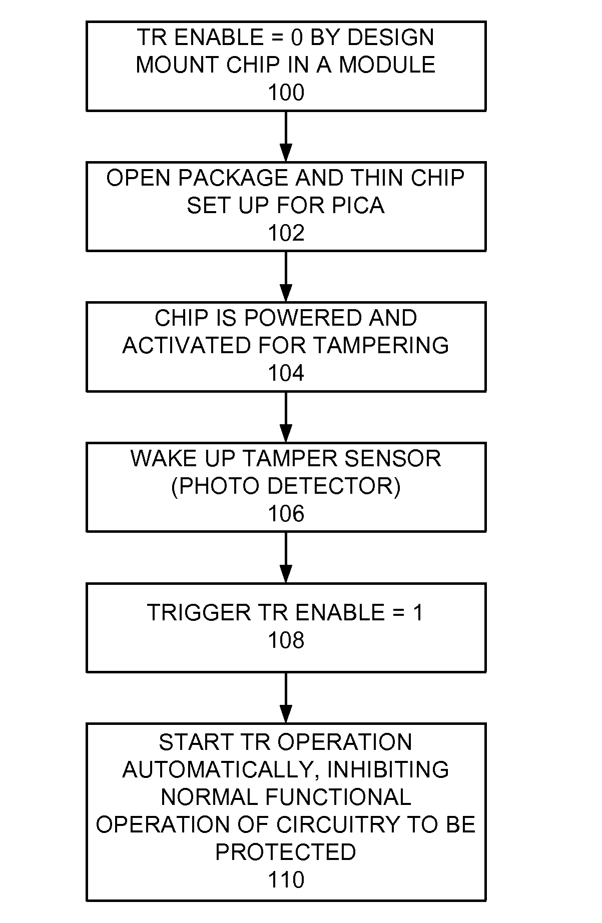
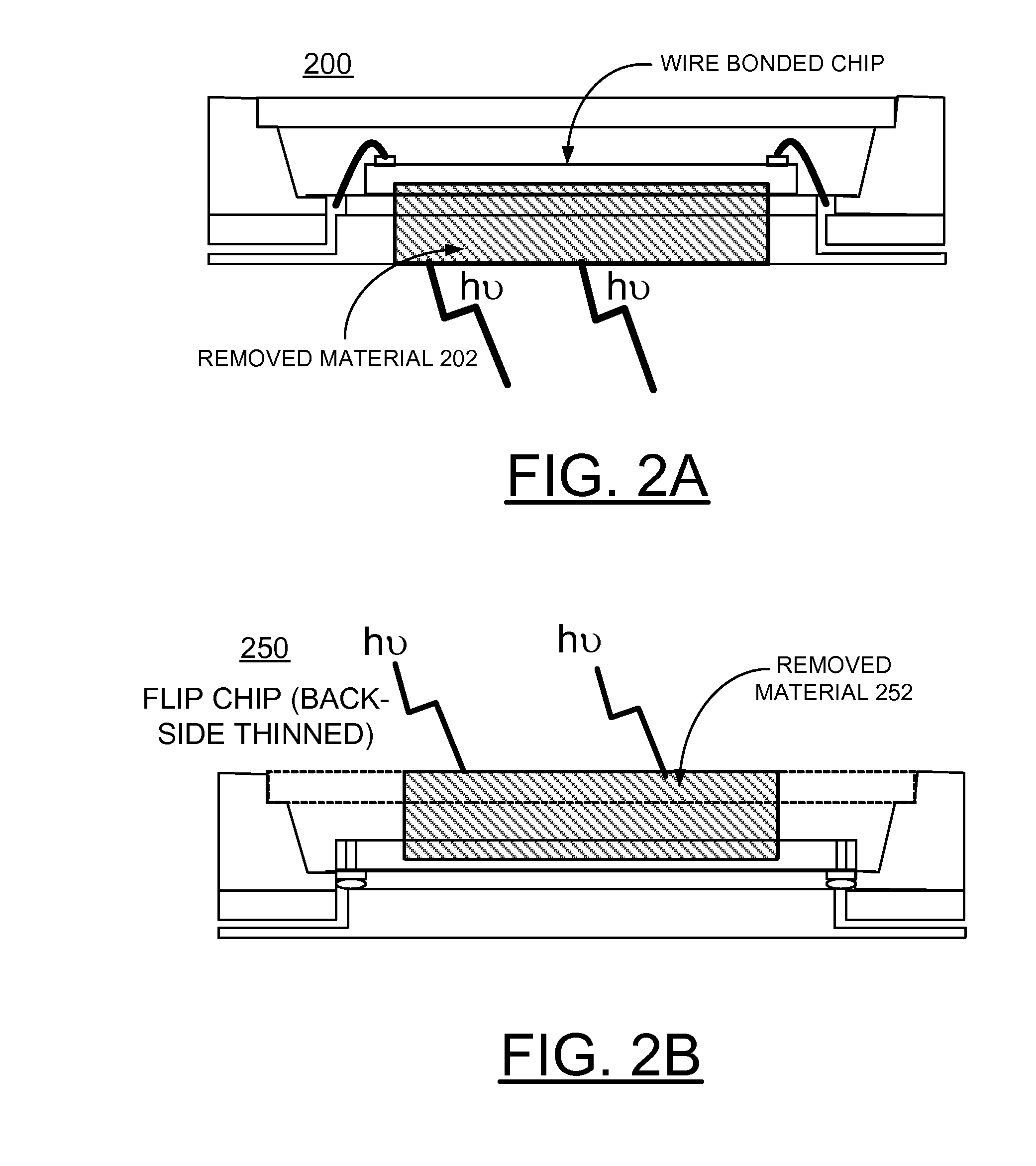
[0032]In accordance with features of the invention, an enhanced method and a tamper resistant circuit for resisting tampering including reverse engineering in a semiconductor chip are provided. The tamper resistant circuit includes three key elements: (1) one or more sensing devices to detect that the package has been opened or removed, (2) generating at least one tamper resistance (TR) enable signal to enable TR operation and (3) disabling at least one circuit block to prevent chip from being fully operational after being tampered.

[0033]Having reference now to the drawings, in FIG. 1, there are shown exemplary steps of an anti-tampering method implemented by a tamper resistant circuit for resisting reverse engineering in a semiconductor chip in accordance with the preferred embodiment. A critical point is that the TR operation should not be triggered inadvertently during normal operation. As indicated at a block 100, by default design, the TR enable signal should always be at logic...


PUM


Abstract

A method and tamper resistant circuit for resisting tampering including reverse engineering in a semiconductor chip, and a design structure on which the subject circuit resides are provided. A sensing device for detecting a chip tampering state is formed with the semiconductor chip including the circuitry to be protected. A tamper resistant control signal generator is coupled to the sensing unit for generating a tamper resistant control signal responsive to a detected chip tampering state. A functional operation inhibit circuit is coupled to the tamper resistant control signal generator for inhibiting functional operation of the circuitry to be protected responsive to the tamper resistant control signal.

Description

FIELD OF THE INVENTION[0001]The present invention relates generally to the data processing field, and more particularly, relates to a method and tamper resistant circuit for resisting tampering such as reverse engineering in a semiconductor chip, and a design structure on which the subject circuit resides.DESCRIPTION OF THE RELATED ART[0002]As used in the following description and claims, the term “semiconductor chip” should be broadly understood to include a semiconductor chip, an integrated circuit, and a semiconductor chip assembly including a package and semiconductor chip.[0003]Major semiconductor companies heavily invest in research and development (R&D), and in the associated intellectual property. Failure to adequately protect intellectual property is very damaging to the semiconductor industry. In addition, a significant military concern associated with placing high technology on the battlefield is the risk of that technology falling into the enemy's hands. Sophisticated en...

Claims


Application Information

Patent Timeline
Patent Type & Authority Applications(United States)
IPC IPC(8): H03K17/78
CPCH01L23/576H01L2224/48091H01L2924/1461H01L2924/00014H01L2924/00G06F21/87
Inventor HSU, LOUIS L.KRUGER, DAVID W.MASON, JAMES S.OLDREY, RICHARD W.
Owner TERRACE LICENSING LLC
Features
  • Generate Ideas
  • Intellectual Property
  • Life Sciences
  • Materials
  • Tech Scout
  • Unparalleled Data Quality
  • Higher Quality Content
  • 60% Fewer Hallucinations
Learn More