Three-dimensional GAN epitaxial structure and manufacturing method thereof

a three-dimensional gan and epitaxial structure technology, applied in the direction of crystal growth process, polycrystalline material growth, chemically reactive gas growth process, etc., can solve the problems of low luminous intensity, difficult control of thickness and manufacturing quality of thin films, and low light emitted by photoelectric elements, so as to achieve easy connection and widen the effect of area

Active Publication Date: 2010-09-16
NAT SUN YAT SEN UNIV
View PDF6 Cites 6 Cited by
  • Summary
  • Abstract
  • Description
  • Claims
  • Application Information

AI Technical Summary

Benefits of technology

[0012]The primary objective of the present invention is to provide a three-dimensional GaN epitaxial structure with a wider area for an electrode to easily connect, so that it is more suitable to be applied on luminous elements.

Problems solved by technology

However, through MOCVD method, it is difficult to control a thickness and manufacturing quality of the thin film.
Thus, when the large-sized thin film of GaN is utilized to form photoelectric elements, light emitted by the photoelectric elements is liable to have a broad range in wavelength, which causes low luminous intensity.
However, due to difference of lattice sizes between GaN and material of the substrate such as Al2O3 or Si, dislocation or defect will be happened easily in initial grown structure of GaN on the substrate.
However, the diameter of the top of the GaN nanopillar is smaller than 1 μm, and thus difficulty in arranging the connecting portion on such small area is high.
However, if GaN rods as described above are applied to luminous elements, the diameter of the top of each GaN rod is too small to form a connecting portion thereon.
Moreover, the additional and needed buffer layer for growing the GaN structure leads to complicate manufacturing processes and time consuming.

Method used


Image

  • Three-dimensional GAN epitaxial structure and manufacturing method thereof
  • Three-dimensional GAN epitaxial structure and manufacturing method thereof
  • Three-dimensional GAN epitaxial structure and manufacturing method thereof

Examples


Embodiment Construction

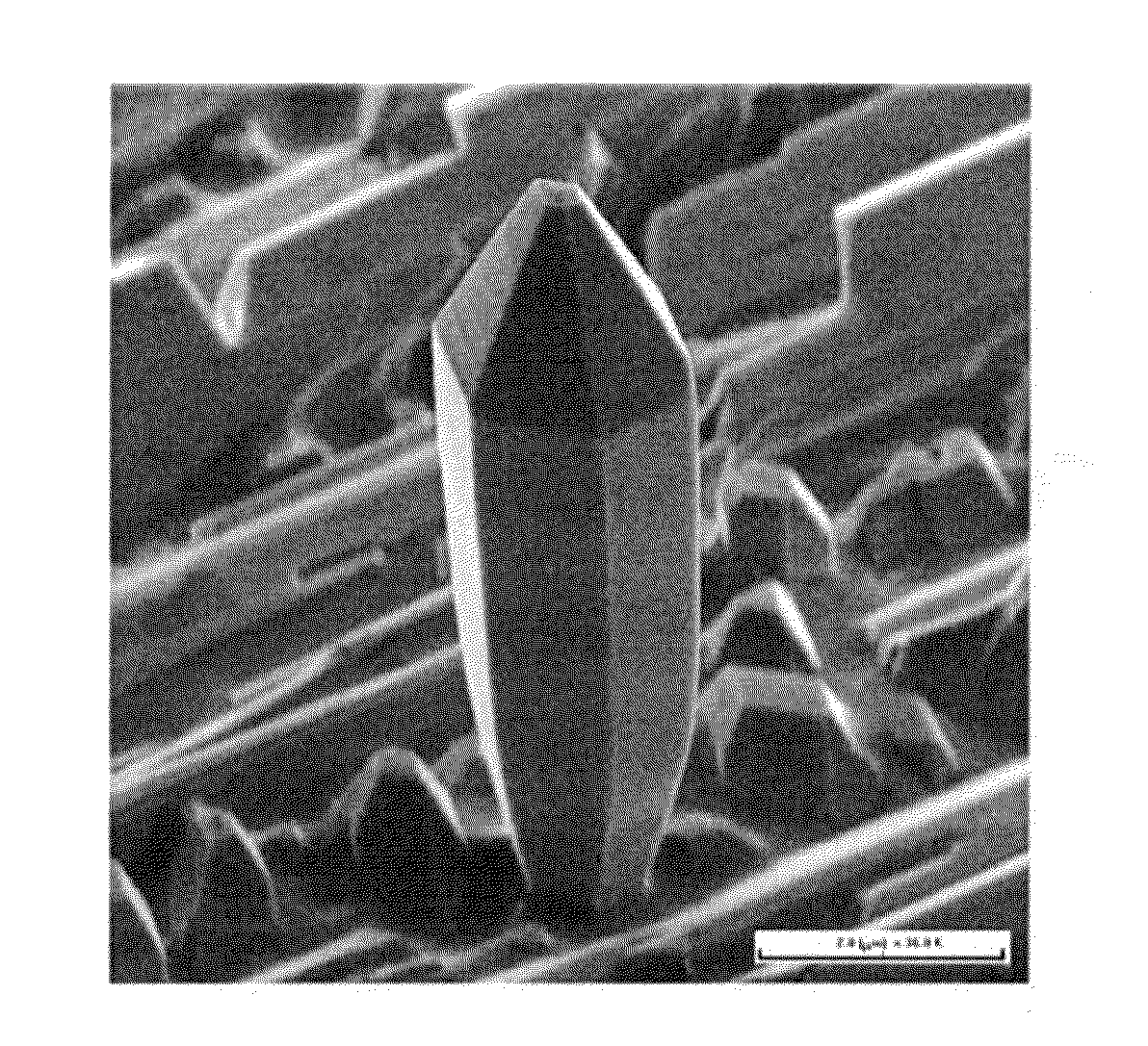
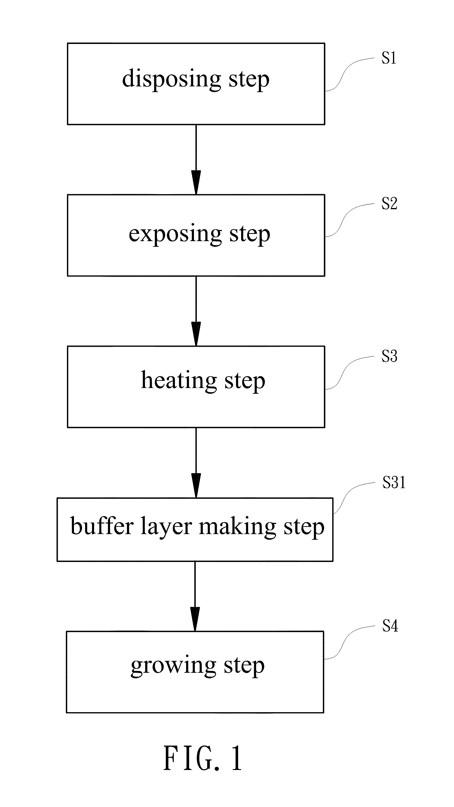
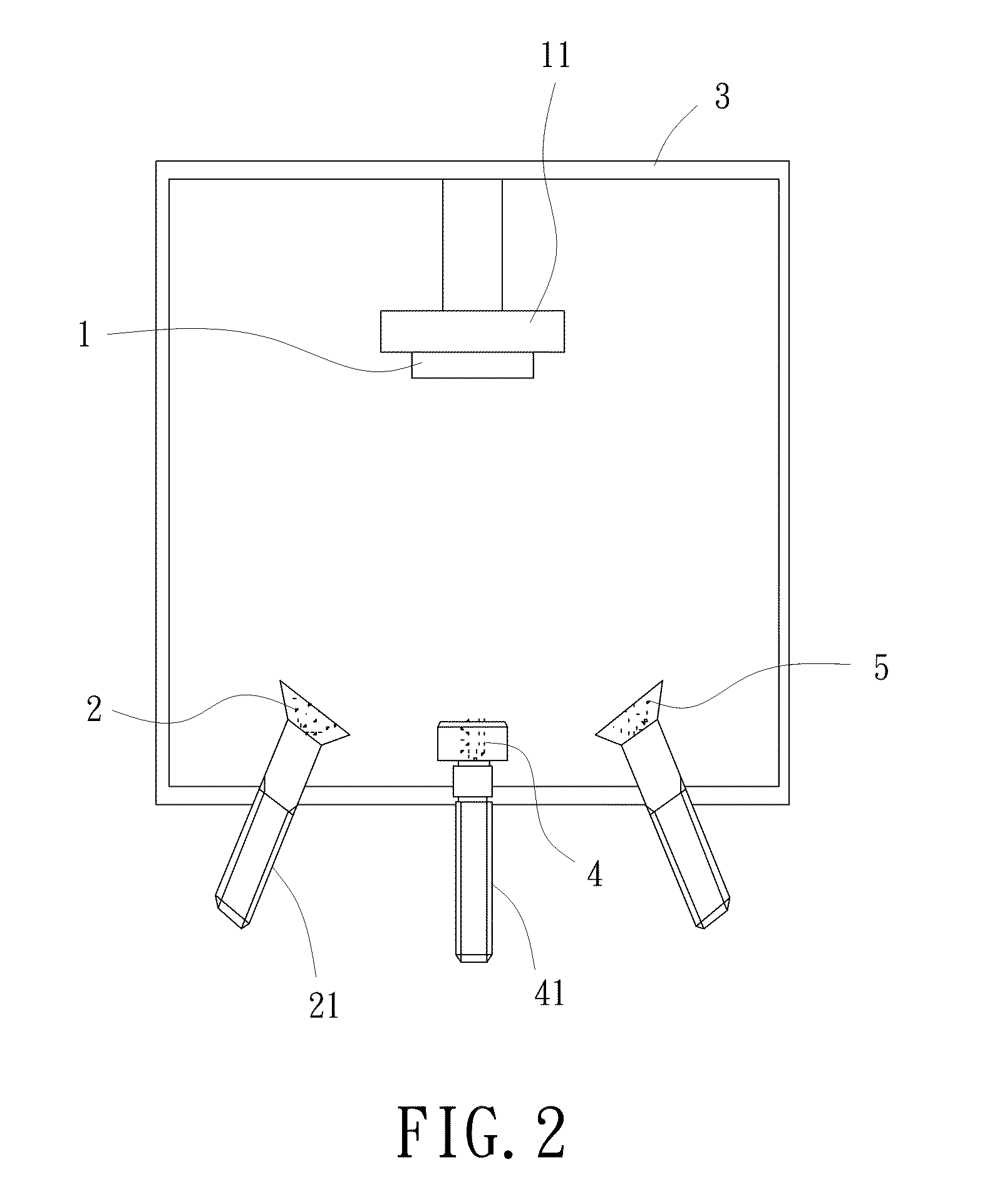
[0030]A manufacturing method for three-dimensional (3D) GaN epitaxial structure of a preferred embodiment according to the preferred teachings of the present invention is shown in FIGS. 1 and 2. The present invention includes a disposing step S1, in which a substrate 1 of LiAlO2 and a source metal 2 of Ga are disposed inside a chamber 3, an exposing step S2 importing N ions generated by a nitrogen source 4 into the chamber 3, a heating step S3 heating up the source metal 2 to generate Ga vapor, a buffer layer making step S31 forming a GaN buffer layer on the surface of the substrate 1, and a growing step S4 forming a three-dimensional GaN epitaxial structure on the substrate 1 by reaction between the Ga vapor and the plasma state of N ions.

[0031]In detail, regarding the disposing step S1, the chamber 3 is connected with an air-extracting apparatus to reach an ultra-high vacuum. Preferably, the substrate 1 is cleaned first by acetone, isopropanol, and deionized water etc. in order fo...


PUM

PropertyMeasurementUnit
temperatureaaaaaaaaaa
angleaaaaaaaaaa

Abstract

A manufacturing method for three-dimensional GaN epitaxial structure comprises a disposing step, in which a substrate of LiAlO2 and a source metal of Ga are disposed inside an vacuum chamber. An exposing step is importing N ions in plasma state and generated by a nitrogen source into the chamber. A heating step is heating up the source metal to generate Ga vapor. A growing step is forming a three-dimensional GaN epitaxial structure with hexagonal micropyramid or hexagonal rod having a broadened disk-like surface on the substrate by reaction between the Ga vapor and the plasma state of N ions.

Description

BACKGROUND OF THE INVENTION[0001]1. Field of the Invention[0002]The present invention relates to an epitaxial nano-structure and manufacturing method for growing epitaxy and, more particularly, to a three-dimensional GaN epitaxial structure and manufacturing method thereof.[0003]2. Description of the Related Art[0004]Conventional manufacturing method for growing Gallium nitride (GaN) structure is metal-organic chemical vapor deposition, MOCVD. For forming a thin film on a substrate through MOCVD method, a carrier gas such as hydrogen (H2) or nitrogen (N2) carries a saturated vapor, which is generated by a metal-organic source, to a chamber to mix with other gases and a chemical reaction is then taken place on a surface of the substrate with high temperature in the chamber, so that the thin film with large area is formed on the surface of the substrate by deposition. Namely, the thin film grows on the substrate gradually when the MOCVD method is processed.[0005]In MOCVD, the carrier ...

Claims


Application Information

Patent Timeline
Patent Type & Authority Applications(United States)
IPC IPC(8): C30B25/02H01L21/205
CPCC30B23/02C30B23/025C30B29/406C30B29/60H01L21/0242Y10T117/102H01L21/0254H01L21/02631C30B25/18Y10T117/1016H01L21/02458C30B25/02
Inventor LO, I-KAIHSIEH, CHIA-HOHSU, YU-CHIPANG, WEN-YUANCHOU, MING-CHI
Owner NAT SUN YAT SEN UNIV
Why Eureka
Try Eureka