Nor flash memory structure with highly-doped drain region and method of manufacturing the same

a technology of flash memory and drain region, which is applied in the direction of semiconductor devices, electrical devices, transistors, etc., can solve the problems of reducing device dimensions and damaging the memory structur

Inactive Publication Date: 2010-09-16
EON SILICON SOLUTION
View PDF4 Cites 5 Cited by
  • Summary
  • Abstract
  • Description
  • Claims
  • Application Information

AI Technical Summary

Benefits of technology

[0010]With the above arrangements and the above manufacturing method, the NOR flash memory structure according to the present invention can have a lightly-doped drain region that is not subject to punch-through during forming the contact hole by etching.

Problems solved by technology

However, there are also problems caused by such reduction of device dimensions.
While the LDD reduces the high electric field at the drain junction and effectively upgrades the reliability of the device, the LDD with shallow junction depth tends to be punched through in the etching process for forming contact hole to thereby damage the memory structure.

Method used


Image

  • Nor flash memory structure with highly-doped drain region and method of manufacturing the same
  • Nor flash memory structure with highly-doped drain region and method of manufacturing the same
  • Nor flash memory structure with highly-doped drain region and method of manufacturing the same

Examples


Embodiment Construction

[0013]The present invention will now be described with a preferred embodiment thereof. For the purpose of easy to understand, elements that are the same in the illustrated preferred embodiment and the accompanying drawings are denoted by the same reference numerals.

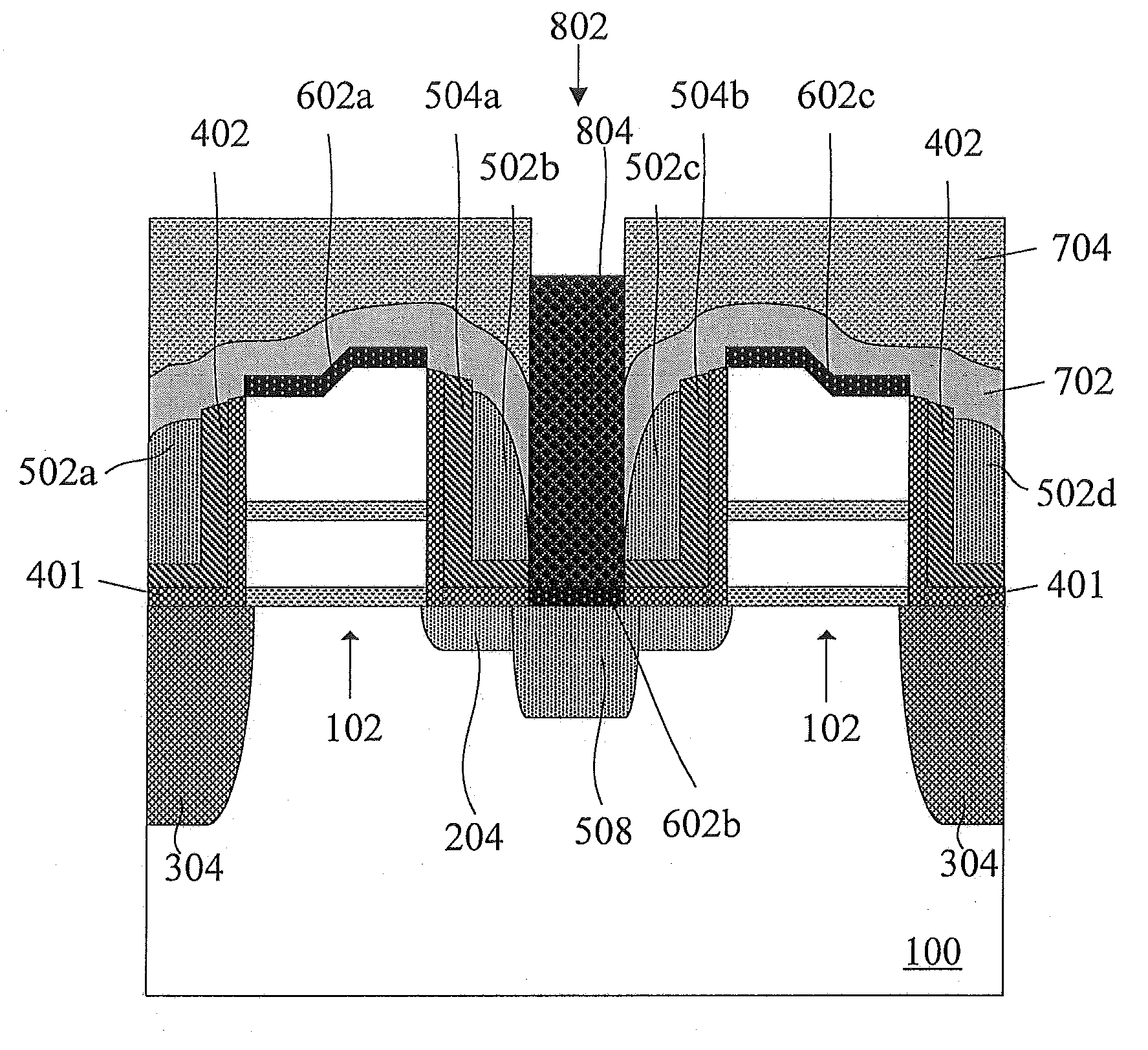
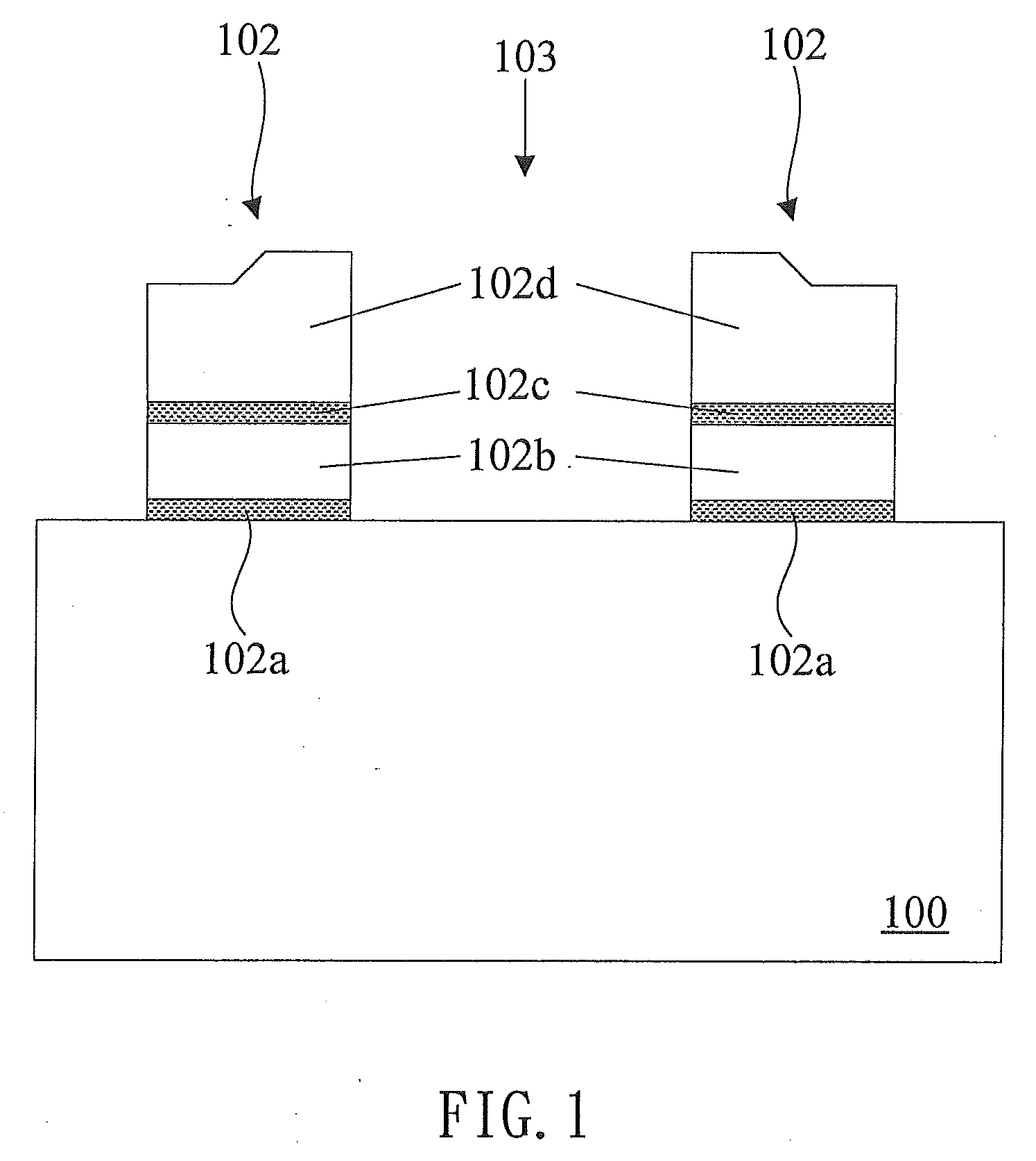
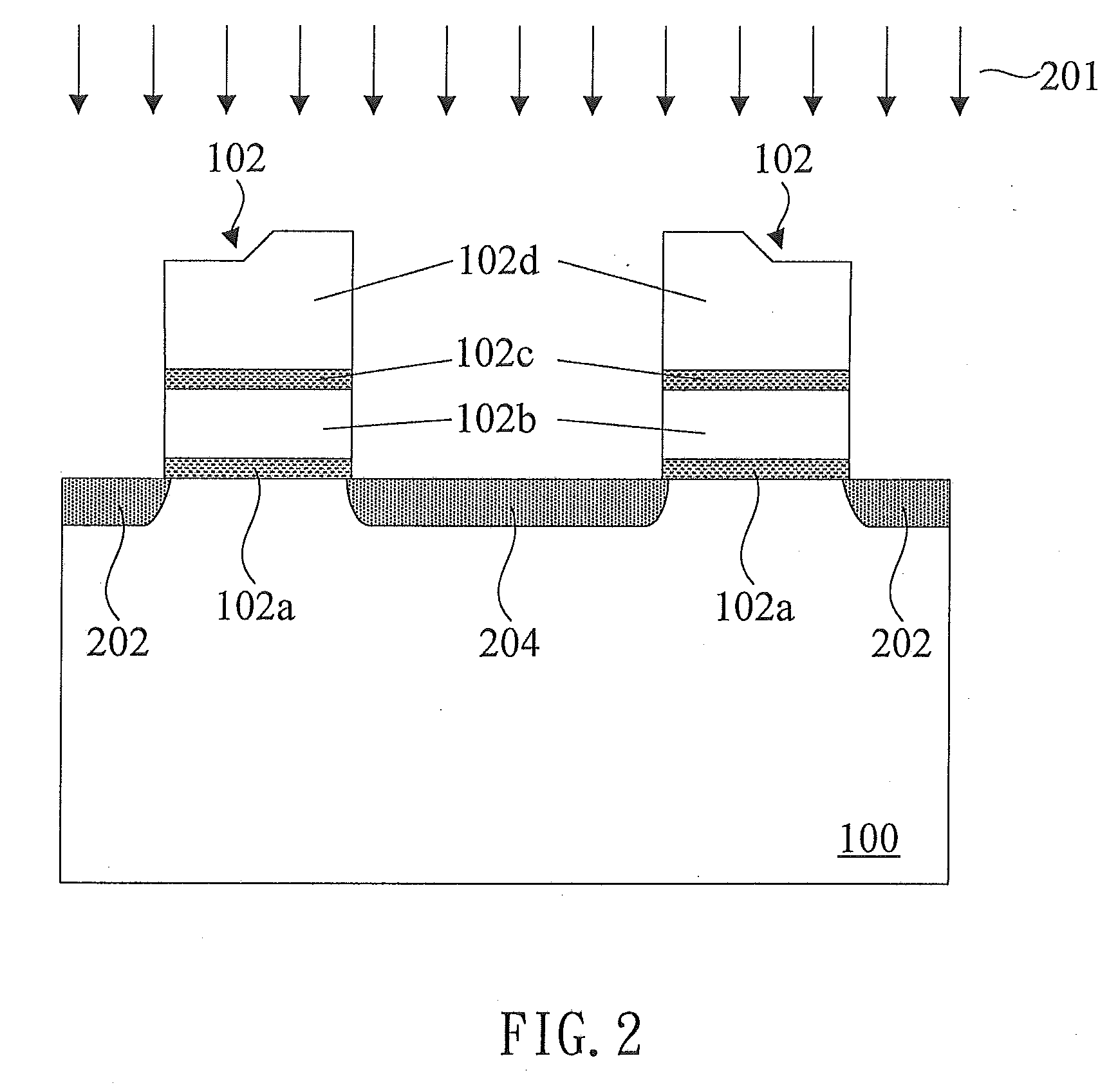
[0014]Please refer to FIG. 1, which is a fragmentary sectioned side of view showing some basic parts of the NOR flash memory structure of the present invention. As shown, the NOR flash memory has a semiconductor substrate 100, on which two gate structures 102 are formed. Each of the gate structures 102 includes a tunneling oxide layer 102a, a floating gate 102b, a dielectric layer 102c, and a control gate 102d. A channel 103 is also formed on the semiconductor substrate 100 between the two gate structures 102. The material for the semiconductor substrate 100 can be silicon, silicon-germanium (SiGe), silicon on insulator (SOI), silicon germanium on insulator (SGOI), or germanium on insulator (GOI). In the illustrated embod...


PUM


Abstract

In a method of manufacturing a NOR flash memory structure, a highly-doped ion implantation process is performed to form a highly-doped drain region to overlap with a lightly-doped drain region. Therefore, the flash memory structure can have a reduced drain junction depth to improve the short channel effect while protecting the lightly-doped drain region from being punched through during an etching process for forming a contact hole.

Description

FIELD OF THE INVENTION[0001]The present invention relates to a NOR flash memory structure, and more particularly to a NOR flash memory structure with highly-doped drain region and to a method for manufacturing the NOR flash memory structure.BACKGROUND OF THE INVENTION[0002]A flash memory is a non-volatile memory, which can maintain the information stored thereon even when no power is supplied thereto. This means an electronic device using the flash memory does not need to waste electric power for memorizing data. The flash memory is also rewritable, small in volume with high memory capacity, and easy to carry. Therefore, flash memories are particularly suitable for use with portable devices. Currently, NOR flash memories have been used not only on motherboards of computers for storing BIOS (basic input / output system) data, but also on mobile phones and hand-held devices for storing system data. In addition, the flash memory offers fast read access speed to satisfy the demands for qu...

Claims


Application Information

Patent Timeline
Patent Type & Authority Applications(United States)
IPC IPC(8): H01L29/788H01L21/336H01L29/00
CPCH01L21/28273H01L29/42324H01L27/11521H01L29/40114H10B41/30
Inventor WU, YIDERLEE, YUNG-CHUNGCHEN, YI-HSIU
Owner EON SILICON SOLUTION
Why Eureka
Try Eureka